Continue to Site

Welcome to EDAboard.com

Welcome to our site! EDAboard.com is an international Electronics Discussion Forum focused on EDA software, circuits, schematics, books, theory, papers, asic, pld, 8051, DSP, Network, RF, Analog Design, PCB, Service Manuals... and a whole lot more! To participate you need to register. Registration is free. Click here to register now.

Photo transistor problem

Status
Not open for further replies.

boylesg

Advanced Member level 4
Joined
Jul 15, 2012
Messages
1,023
Helped
5
Reputation
10
Reaction score
6
Trophy points
1,318
Location
Epping, Victoria, Australia
Activity points
11,697
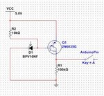
This is a really basic circuit but I am having trouble with it none the less:


Q1 is actually BC517 on my real circuit and D1 is a SHF309FA-3/4 or alternatively a photo diode I got from ebay but am unsure as to its identity.

Regardless I am getting a roughly 1V differential on the base of the BC517 when I shine a TV remove into the photo diode.
But I am only getting a milli-volt differential on the emitter of the BC517. So why is the darlington not amplifying the current and the voltage?

How do I get a 2-3V differential out of the photo-diode?
 

Would you mind to draw the circuit with correct component polaritiy?

The basic design fault is lack of a load resistor. The darlington transistor will be possibly turned on by photo transistor leakage current and surely by ambient light.

I guess, the secret behind your "measurement results" is that you connect a multimeter or oscilloscope (10 Mohm load) when measuring the base voltage and removed it during the output measurement. Should give you a rough idea what to do.

PhotoTrans.jpg

This works better but it is still only a 1.2V max swing - I replaced BC517 with BC516.

But then replaced R1 with a 1M and then a 10M resistor and it finally breaks the 2V swing barrier - much better.

I find it rather surprising that it has been impossible to find an example of interfacing a photo transistor with an arduino digital pin. There are plenty of examples interfacing them with the analog pins but that is not what I wan in this case because I need the photo transistor to trigger an interrupt.
 

Photo diode/transistor polarity still wrongly sketched after switching to PNP transistor. I presume it's only the schematic.

Operating the transistor in common emitter configuration is basically a good idea. R2 is useless as shown. Load resistance in my post refers to a resistor between darlington base terminal and ground, respectively between base and emitter in the new schematic.
 

I have been assuming that the symbol of a phototransistor is arranged the same way as the symbol of a LED - obviously I am mistaken.

Just looked at a data sheet. I have the anode connected to Vcc and the collector to the base of the BC516.
 

Why don't you look at Photo Diode in Google? It shows that it can be used in two different ways:
1) Forward Biased like you have it. Then it is a tiny solar cell that produces a very low voltage like you have. Your darlington is an emitter-follower with NO voltage gain so its output voltage is low.
2) Reverse Biased. Then light causes it to leak a small current but your emitter-follower has no voltage gain and again produces a very small voltage.

If you use a photo-transistor and connected it to have voltage gain then its output voltage will be much higher than a photo diode.

EDIT: You also need to look up Emitter Follower in Google to see its voltage gain.

Thanks mate.

I seem to have this mind set where I am focused on getting positive output from positive input but forgetting about this emitter follower thing that does not have high voltage gain.

I can immediately see now, with the BC516 version of my circuit, that I have a common emitter amplifier, that does give voltage gain but with no inversion as with an NPN version of it - exactly what I want.
 

I made a mistake.
When a photo diode is used as a tiny solar panel then you feed it no bias voltage. Its output voltage and current are too small for a transistor or darlington so an opamp is used to amplify it.

A common emitter transistor is an inverter. The PNP inverts and the NPN inverts.
Your PNP circuit wrongly has the photo diode forward biased with an extremely high current (it is in series with the forward biased base emitter of the PNP transistor with nothing limiting the current).
 

What value resistor would you recommend? I guess it can't be too high otherwise I will loose the high output voltage level.

The phototransistors never seem to generate much voltage or current even with an IR LED on top of them so I figured I probably didn't need a limiting resistor.
 
Last edited:

Your circuit with the PNP darlington has the photo diode forward biased which is NEVER done with a photo diode. The current through it is MASSIVE and is will burn out. It is not a photo diode like that.
Reverse the polarity of the photo diode (and replace it and the darlington if you powered the circuit with them burning out) then it will conduct some small leakage current when it has some light and the darlington will amplify the small current. The darlington might stay turned on in the dark by "dark current" so add a 1M resistor from base to emitter of the darlington.
 

Photodiodes are ALWAYS reverse biased and operate as current sources with light input. All diodes have Maximum capacitance at 0V and decreases with reverse bias. In this case 5pF max. But this only relevant for maximum speed >100kHz~ 1MHz because the Miller Capacitance of your transistor swamps the diode. ( better choices with trans-impedance op amps, TIA and other devices)

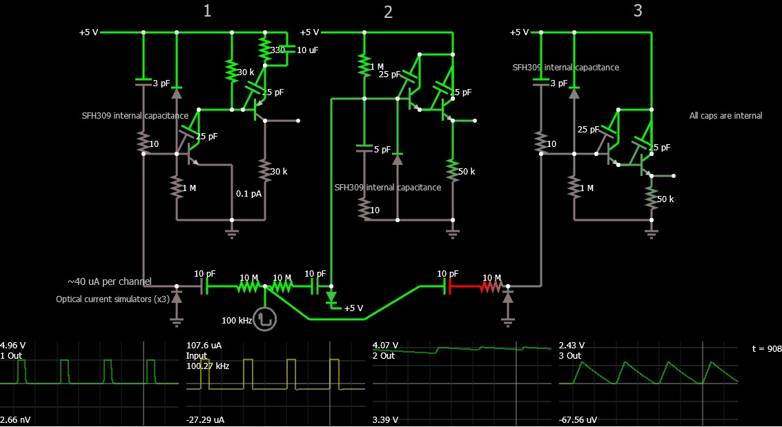
3 examples below show low level input switched current is simulated with high voltage and high R.

The best voltage gain with high impedance output is a two stage CE amp.
Choose base/collector ratios of 30 or so for good bandwidth and gain.
5222495000_1442004416.jpg

My design above
The emitter follower has the advantage of lower output impedance and higher input impedance but no V gain.
The common emitter, (CE) followed by emitter follower suffers from slew rate limiting of Miller capacitance.

But the 2 stage CE with NPN, PNP gives two inversions, thus non-inverting , more voltage gain and output impedance is Rc of 3K is low enough to easily drive logic.

Note that inversion is not a problem as reverse biased to ground with 1M pullup would also invert input signal if you wanted only 1 stage.

Sensitivity and more gain can be improved using a null offset Op Amp as a TIA with a comparator.

Simplified SImulation Photodiode cap removed and important R Ratios
needs java approval

For remote controls they use pulsed carriers so the Rx has AGC BPF and far better range.

Note also I added the Miller Capacitance typical for PN2222 and your Darlingtons.
 

With ~120 uA optical current split into 3 different designs for ~40uA , you can get the optimum gain and bandwidth for this configuration with 2 BJT's

Each device shown is hFE =100 declining to 50 to 20 to 10 when saturated, and the R ratios I have chosen from Rb/Rc for each stage are important for optimizing gain , slew rate and symmetry of pulse width.

As you see there is 5V output swing with a current gain of minimum 1000x (out of 10k) in this configuration before loading affects waveform symmetry.

So if you want to try that,, test my "falstad" link for giggles and kicks and change #1 out Rc to 100 Ohms for 50 mA out and notice the pulse width and voltage and rise time on 1st trace..


If 40uA into 1M is 40uV and #1 Rc out is 5V,
what is the voltage gain?
 

Status
Not open for further replies.

Part and Inventory Search

Welcome to EDABoard.com

Sponsor

Back
Top