sapphire_2010
Member level 5

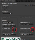
How to calculate critical trace length on a PCB, in both time and frequency domain method? Is there any calculator available?
I found below link as a reference, but wondering if the formula remain same whether my trace is in outer or inner layer?
I found below link as a reference, but wondering if the formula remain same whether my trace is in outer or inner layer?