Continue to Site

Welcome to EDAboard.com

Welcome to our site! EDAboard.com is an international Electronics Discussion Forum focused on EDA software, circuits, schematics, books, theory, papers, asic, pld, 8051, DSP, Network, RF, Analog Design, PCB, Service Manuals... and a whole lot more! To participate you need to register. Registration is free. Click here to register now.

PCB grounding error in Altium

Status
Not open for further replies.

arr_baobao

Full Member level 2
Full Member level 2
Joined
Nov 1, 2011
Messages
134
Helped
0
Reputation
0
Reaction score
0
Trophy points
1,296
Activity points
2,317
Hi,

i had encounter the problem below in my PCB design using altium software. I alrdy connect both the red polygon to GND in for the circuitry in bottom right. But why there is still a white line between 2 via pad in the polygon, i know that this mean that both are not connected to ground. But why?
Anyone can advice? IMG_2226.jpg
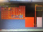
 

It doesn't mean that they are both not connected to GND, it means that there is no connection between two objects within one net.
As for your case, I don't see the bottom GND plane. Do you have a GND polygon? Is it shelved? To get rid of that error the polygon must be filled (restored and visible). Or have a direct connection.

thanks. how to set the bottom layer as ground?
 

As far I as know, you cannot make external layers (top and bottom) as plane layers, instead of that you should place polygon plane with the desired shape (you can just make a polygon repeating the PCB shape with small gap between the poly and the board edges) and connect it to GND.
 

As far I as know, you cannot make external layers (top and bottom) as plane layers, instead of that you should place polygon plane with the desired shape (you can just make a polygon repeating the PCB shape with small gap between the poly and the board edges) and connect it to GND.

i alrdy did connected my all my polygon to ground.
 

I don't see the bottom GND polygon. If your bottom layer is empty, thus there is no connection.
 

Is there any connection in bottom layer? Just putting vias will not make conection, you need to have some trace or polygon in other layers where you intend to connect these vias to.

What is your layer stackup?
 
Is there any connection in bottom layer? Just putting vias will not make conection, you need to have some trace or polygon in other layers where you intend to connect these vias to.

What is your layer stackup?

thx. alrdy add a layer of ground polygon
 

Status
Not open for further replies.

Part and Inventory Search

Welcome to EDABoard.com

Sponsor

Back
Top