thambiTeaInnumVarala
Newbie level 3

Hi,
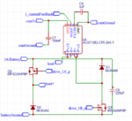
I am making a half bridge power amplifier that operates at 24 V.
The bridge has to supply around 3A current to an inductive load (10mH)
The bridge will be controlled using 20kHz PWM from a microcontroller.
I have put a ACS712 current sensor in the load path to give feedaback to the microcontroller.
There is a IRF9Z24 P FET at the top and a IRFZ44 N FET at the bottom.
Both are driven by a single MC34125 Gate driver IC, which has a 12 V power supply.
The gate driver is connected to the microcontroller through a HCPL optocoupler.
I have maintained 80mil track width for the 3A paths, from a online track width calculator.
I have put necessary decoupling capacitors for the optocoupler and the gate driver ic.
There are 2 copper filled ground planes on top layer and bottom layer that I have not shown in the pcb schematic for visibility.
I have made a schematic and circuit diagram that i have linked here.
Pl suggest any modifications or pointers that will improve the circuit.
Thanks.
TIV


