Welcome to our site! EDAboard.com is an international Electronics Discussion Forum focused on EDA software, circuits, schematics, books, theory, papers, asic, pld, 8051, DSP, Network, RF, Analog Design, PCB, Service Manuals... and a whole lot more! To participate you need to register. Registration is free. Click here to register now.
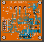
The placement and routing seems fine, although I could recomend keep away components from screw's holes, not only to avoid the possibility of the screwdriver hit them, but also to extend the path of the ground plane. In addition, there are obviously other minor aesthetic aspects, as designators with size and different orientations.
There is no schematic so I cannot say much about how it's laid out (although it looks good)
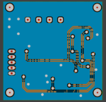
Top tracking layer:
1) Mounting holes - they look too small. (hole size set wrong?)
2) Be aware that if using screws into a metal standoff then you will short the board to the case, the resist cannot be used for isolation. (create copper gap bigger than screw head.)
3) The cap next to SH2 - move further away, terminal blocks can change in size easily depending on supplier - keep a good gap around them. (See #8)
4) Bear in mind the return current paths, so for instance - for IC3 - how is it getting it's gnd (B-)? (EMC)
Then follow the gnd (B-) path from say C7 to the GND pin of IC3 - is this a big loop? if so close it.
Adding stitching vias may help to do this, these join the top copper to the bottom copper.
5) Also rotating C7 so the GND is at the top gets it closer to the GND source & reduces the path. (see #4)
6) Ditto R8. (see #4)
7) Between R15\R16 there is a very thin bit of B- copper, never consider this as an adequate path for a return current no matter how small - so it will go up and over the B+ terminal pin, making it a long path, move R15 up a bit so that this can be made thicker.
8) The track under U2 - move to the right a bit so that the copper can be thicker, if you use screws then it may short the pins of U2 - its very close to the mounting hole.
Bottom tracking:
To be picky on the groundplane - join the gaps.
1) The RH track, move further to the right so that the copper between it and the next track can connect.
2) Pull the bottom segment of the bottom track down further so that the copper can flood under the via that is above R11
3) The track connecting to the via\C7 has a mitre in it, mitre it further down so that the spark gap looking copper points can join well.
4) Are your thermal relief spokes thick enough for the current that will flow through them?
Silkscreen:
1) Make all component names the same size text. (readability)
2) Decide which way is up when in the enclosure and then make text read
1st) Left to right. (preferred)
2nd) Bottom to top. Not upside down. (readability)
3) Connector names & text can be bigger. (readability)
4) Possibly put IC names near pin 1, be consistent - like always put the name above the component unless not possible.
5) There should be a 5 thou gap between silkscreen text and pads - never over pads.
6) Do not place component names over vias - they will have holes so the text may be unreadable.
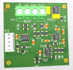
7) There is no identification text - what is it and who's is it? What version, model, revision is it?
I'm being finicky and your board is fine and will likely work fine - however Im just passing on some good practice advise to help with EMC, assembly and repair.
Thank you both,
Very detailed and in depth report there MAttylad, Thanks for taking the time, I will take your comments on board and make the alterations to the PCB, Yes the Mounting holes are small and incorrect, I will change the parts you mentioned around and add some more via stitching. It's part of a project that I'm working on basically it measure 0-20V 0-70amps in either direction and output a signal to indicate which way the current is flowing through the shunt with SD card logging, I normally use through hole components but thought I'd give SMD a try and get the PCB'S made in a fab house. I know some of the silk screen stuff is odd size but this will be all tidied up towards the end.
It's good to get some input and good advice has I know PCB design is a black art in it's self
Just an additional advice:
Keep grounding plane apart from the PCB outline to avoid short circuit the board GND with the chassis of the case and/or other devices referenced to a different potential.
The board does not carry 70amps, There is an external shunt that carries the current, The 0-75Mv comes in on JP2 and then the op-amp are set up to boost the voltage and convert the negative signal into a positive signal when the current is been drawn in the opposite direction . I will modify the Polygon so it does not go to the edge
This site uses cookies to help personalise content, tailor your experience and to keep you logged in if you register.
By continuing to use this site, you are consenting to our use of cookies.


") . I will modify the Polygon so it does not go to the edge
. I will modify the Polygon so it does not go to the edge