anpiri
Newbie

- Joined
- Jan 13, 2025
- Messages
- 1
- Helped
- 0
- Reputation
- 0
- Reaction score
- 0
- Trophy points
- 1
- Activity points
- 22
Hi all,
I am working on a project that requires 8 channel signal being converted into 8 differential signal using ‘Balun’s’ or transformers. This is because I need to connect 8 antenna's that are single ended to an FPGA ZCU208 evaluation board that has differential inputs. I am not experienced with RF components, and so I lack knowledge to ensure this conversion is done correctly. Any help regarding isolation, trace sizes and general board design would be appreciated.
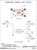
I have made a basic 2 layer PCB design based on a schematic I found online for a transformer evaluation board using the components;
1) TCM2-63WX+; 1:2 CORE & WIRE Transformer, 30 - 6000 MHz, 50Ω | TCM2-63WX+ | Mini-Circuits
2) 0.5 PF capacitor
3) SMA edge connectors for the input and outputs. I designed the footprint for this SMA myself and based it off the mechanical dimensions.
My question is, what other things should I be thinking about to reduce crosstalk and any other problems? Trace width? I know we expect to be using around 5Ghz signals. Any advice regarding current spacing and trace widths would be appreciated.
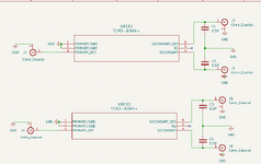
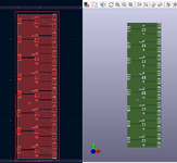
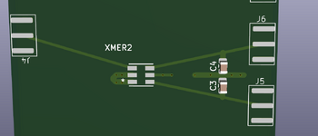
My schematic has been included where it is 8 of the same circuit, and the current pcb layout included as well. Would one ground plane and one copper plane be good enough? Should the signal trace be thicker than all?
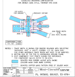
There is the PCB layout for the evaluation board provided, so I tried to replicate it and place 8 on the same pcb essentially as in a second design (image provided of close up pcb designed).
FPGA eval board link: https://docs.amd.com/v/u/en-US/ug1410-zcu208-eval-bd
Transformer link: https://www.minicircuits.com/WebStore/dashboard.html?model=TCM2-63WX+
Transformer eval board PCB layout: https://www.minicircuits.com/pcb/98-pl380.pdf
