Continue to Site

Welcome to EDAboard.com

Welcome to our site! EDAboard.com is an international Electronics Discussion Forum focused on EDA software, circuits, schematics, books, theory, papers, asic, pld, 8051, DSP, Network, RF, Analog Design, PCB, Service Manuals... and a whole lot more! To participate you need to register. Registration is free. Click here to register now.

Paralelling mosfets for harmonic reduction

Saltwater

Member level 4
Member level 4
Joined
Aug 30, 2015
Messages
71
Helped
0
Reputation
0
Reaction score
0
Trophy points
1,286
Activity points
1,922
Hi,

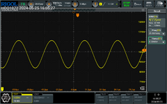
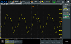
I'm trying various methods to build a common emitter class A amplifier for home studio use. And I noticed the IRLZ Hexfets im using have a decent amount of harmonic distortion say about 1-3% on the first harmonic. I'm using about 20V supply voltage and running the fets at about a 4v output.

This is on one transistor. "Keeping it in the common emitter spirit" Would it make sense? To have paralel mosfets to keep a lower resistance, and higher output power for the same pre- amplifier gain. Or is this a paradox and will the results actually be worse?

RigolDS9.png
 
I don't have feedback on the amplifier. Main reason is that the total inductance is relatively low for audio, so my guess is that I wouldn't have to for linearity as long as the power supply has sufficient noise rejection. Especially the Pre-amp (Same topology with a single plugin transistor 2n2222/ BC550) is as sensitive it shows signals produced by my converter. As of now its slightly better tuned than these screenshots where.
 

Attachments

  • niquistm4176preamp0.png
    niquistm4176preamp0.png
    154.4 KB · Views: 31
  • niquistm4176preampsq0.png
    niquistm4176preampsq0.png
    162.4 KB · Views: 33
  • cappy2.png
    cappy2.png
    208.7 KB · Views: 33
Both BJTs and FETs have a square law behaviour for output current with input voltage. So to minimize distortion the bias must be held constant.
This is best done with either low gain as in power Amps or high negative feedback with current sources as in pre-amps.

While emitter followers and source followers need a CC load rather than a fixed R to keep bias constant that varies source impedance..
 
Last edited:
Thanks for the replies, I'm feeling a bit more confident this may yield some results. Also maybe as a means to stabilize the bias voltage to use a little feedback for the pre-amp.


Cut.png


The circuit under test is alike without the second transistor. Since the resistance effectively halves there would be more gain. But no where I can find what it would do to suppress the first harmonic?
 
Last edited:
Hi,

no part values, no voltages.

I better leave this thread ... to avoid to annoy by asking for complete informations again and again..

Klaus
 
Klaus, it's 20V through a IRLZ34NPBF HEXFET. But that may change. And is higly subject to environment variables and the point.
Edit: I got reprimended before for thanking. Do you want to simulate the circuit?

Anyway,
It takes a bit of resource to manouvre the hot parts in order to fit, but it will be made. In satturation mode this makes no sense at all, but maybe,

R2 = R-R,
C Para = C+C
Vgm = 20v / 4 = 5v will be Vgm = 20v / 8 = 2.5v
 
Last edited:
There are no inductors added to the circuit?
I read "Main reason is that the total inductance is relatively low for audio,"

Can you show your schematic and layout?

Does a 10 kHz square wave look the same?

Perhaps it is your speaker inductance.
--- Updated ---

I tried to simulate your distortion and failed from wild guesswork.

1724690926055.png
 
Last edited:
Hi,

Sorry to confuse you, I ment the inverse of the capacitance. For lack of a better word. I have about exactly 1.1uf added to the pre-amp circuit. So it should be well RF.
I see examples where the circuit sags in the high end(where people suggest using feedback amplification to solve for the bandwith). Here it is continually showing the used converter ringing at about a 441 niquist frequency.
RigolDS12.png

For the altered circuit with 3 of the HEXFETS, its a bit of a harder beast to maintain a stable temperature coefficient for. After this was settled the results with no load looked sligtly better but far from rational.
RigolDS11.png

After loading it down with a capacitor and a driver, I tuned the power to look best. Offcourse it has way more power but with great power comes great distortion.
So.. Measured driver side.
RigolDS16.pngRigolDS17.pngRigolDS18.png


The problem seems to be the ideal spot for the input signal is dead center in the voltage range, or even lower the results are better. There it starts to conduct heats up and it runs away, at all if not most levels. In my case its in either form not allowed to sustain the sweet spot of the transistor.
 
Last edited:
Dr. Peter Nyquist forgives you.

But this 441 Hz Sawtooth has a 25 kHz resonance which looks to be more than the BW of the signal from looking at the risetime in 6 cycles of 25 kHz
The load resistor is also a damping R, so no load has the highest Q which is a tradeoff with efficiency by raising RdsOn or lowering Vgs.

The ramp time increases on transformer k < 1 and deadtime as well as choice of FET for RdsOn*Coss with ratios on Miller and Gate Capacitance.
Your former plot and recent plot .
1724775972292.png
1724775411808.png


Here I simulated with discrete FET C's and RdsOn to create a 5kW = 70V*70A inverter using NO Deadtime although 48% d.f. works slightly better.
However, FET power increases . Here 5.3kW pulse in < 75 ns every 10us = 40W Avg. for 3.2% losses.

1724776388632.png
 
Must have seen that word a thousand times, I will correct for the better word.
It,s classed as an ESS Sabre 32 Ultra. Cant find the specific part but pulling one up. From guess work I thought those where FIR patterns doing a BLEP or BLIT.
It has a FIR filter, as you mentioned 25KHz, may be the correct number. It's supposed to be held at a 100MHz base clock.
You can see the sine wave is purist, the other one is a square wave.

I don't understand completely. Assuming if the resistance is lowered the circuit will be held at a higher cut off frequency. As well as affecting the charge time of the transistor? So if I have 20² its going to attempt sinking 400W? 🤒 That may require a design change to implement, where the resistor is at the negative potential to ground side.

So i was wondering if that is the reason it likes to be at 1 volt, because of the 1.3 amp? The difference in power is actually not that big. Discounting the driver must have loaded it.
 

LaTeX Commands Quick-Menu:

Part and Inventory Search

Welcome to EDABoard.com

Sponsor

Back
Top