Welcome to our site! EDAboard.com is an international Electronics Discussion Forum focused on EDA software, circuits, schematics, books, theory, papers, asic, pld, 8051, DSP, Network, RF, Analog Design, PCB, Service Manuals... and a whole lot more! To participate you need to register. Registration is free. Click here to register now.
No, having a chamfer on the corners of the IC does not mean you have to do that to the pads.
Plain rectangular pads work fine, bullet shape pads work fine.
Square pads? I'd do them rectangular not square.
Make a rectangular pad at least L x b for each pad. A better pad would be L + 0.004" by b + 0.004", with the resist opening L x b. You can radius the inside part of the pad if you desire, but it is not necessary. With modern PCB tools, you can make any geometry pad that you want.
The drawing that is presented in the datasheet is not always the recommended dimensions for the footprint, but often represent the dimensions of the component itself, therefore you should extend a little the land patterns on this case. Consider the fact that according to current standards, for the same component it is possible to draw slightly different footprints optimized for distinct assembling processes, or rather, the same footprint with varying margins.
My plastic model will be made of PLA or ABS material having 1.5mm thickness.
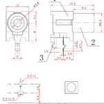
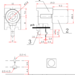
So, total height is 13.2+1.5=14.7mm from pcb.
My switch is having 14mm height from pcb.
So, should I reduce the thickness of model and/or I reduce height by doing this:?
I will push Av connector little outside of pcb so that the block will on outside of pcb.
Will this cause any problem?
I will change pcb hole only size for av connector.
I found I can reduce size by 1.4mm (by scaling image and measuring distance).
Switch head will 0.8mm from case[14-(13.1+1.5-1.4)]=0.8mm.
This site uses cookies to help personalise content, tailor your experience and to keep you logged in if you register.
By continuing to use this site, you are consenting to our use of cookies.