Continue to Site

Welcome to EDAboard.com

Welcome to our site! EDAboard.com is an international Electronics Discussion Forum focused on EDA software, circuits, schematics, books, theory, papers, asic, pld, 8051, DSP, Network, RF, Analog Design, PCB, Service Manuals... and a whole lot more! To participate you need to register. Registration is free. Click here to register now.

Output voltage very low

FreshmanNewbie

Advanced Member level 1
Joined
May 10, 2020
Messages
437
Helped
0
Reputation
0
Reaction score
3
Trophy points
18
Activity points
4,333
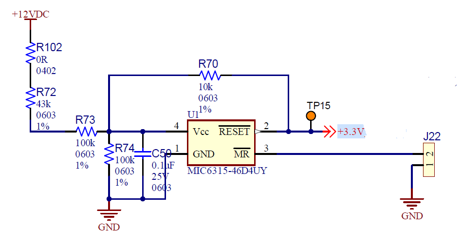
This is the IC that I am using.

1702301347527.png


I am getting 0V at the TP15, when +12VDC is given.

Anyone can expplain why it is
 
Last edited:
What´s the voltage at each other pin w.r.t. GND?

Hint: use a scope to see what´s really happening. ;-)

btw: are you talking about simulation or real circuit?

Klaus
--- Updated ---

Added:
Oops, no scope necessary..
 
What´s the voltage at each other pin w.r.t. GND?

Hint: use a scope to see what´s really happening. ;-)

btw: are you talking about simulation or real circuit?

Klaus
--- Updated ---

Added:
Oops, no scope necessary..
1. Voltage at pin 4 = 0.8V
2. Voltage at pin 2 = 0V.

It is a real circuit.
 
Hi,

shurely there is not 12V at pin4.

What voltage did you calculate for pin#4? Show your math.

Klaus

added:

Debugging:
When the ouptut of an IC is not correct:
* then the first idea should be: Are all the inputs correct?
And with "all" I really meant "all".

This also means pin#3 ... because if it erroneously has the wrong sate it also has impact on the output.
And it also means pin#1. And measured at the very IC pin. This measurement - for debugging - is very important on a real circuit. I´ve seen many fails because of bad soldering.

Klaus
 
Last edited:
Hi,

shurely there is not 12V at pin4.

What voltage did you calculate for pin#4? Show your math.

Klaus

added:

Debugging:
When the ouptut of an IC is not correct:
* then the first idea should be: Are all the inputs correct?
And with "all" I really meant "all".

This also means pin#3 ... because if it erroneously has the wrong sate it also has impact on the output.
And it also means pin#1. And measured at the very IC pin. This measurement - for debugging - is very important on a real circuit. I´ve seen many fails because of bad soldering.

Klaus
I am not saying there is not 12V at pin 4. I am saying the 12V is there present at the top of the R102 resistor. But only 0.8V at the pin 4 of the IC.

I am not calculating. I am testing the circuit in the test bench.
 
You have 143K in series with input severly crippling regulator to work. It may not startup.
due to input RC and effects on reset fdbk.....

Where did this application circuit come from ?

Use a zener to drop the Vin to part.


Regards, Dana.
 
You have 143K in series with input severly crippling regulator to work. It may not startup.
due to input RC and effects on reset fdbk.....

Where did this application circuit come from ?

Use a zener to drop the Vin to part.


Regards, Dana.
Can you please tell me why the 143k in series is not helping?

How alternate method will help? Where should I put the zener?
--- Updated ---

You have 143K in series with input severly crippling regulator to work. It may not startup.
due to input RC and effects on reset fdbk.....

Where did this application circuit come from ?

Use a zener to drop the Vin to part.


Regards, Dana.
Can you please tell me how does the IC not supposed to start-up with this 143k combination? Anyway, the input voltage should be available at the Vcc pin, right?
 
Note the 143K and worst case 15uA power drain results in only a ~ 2V drop
into regulator, eg 10V applied to reg input, hence violating its 6V max. Note you
are assuming the V divider action works as a V divider, but you have no insight
into reg input behaviour.....

12V >> Zener >> Vcc 6315 would be wiring. You have to work out
Vz tolerance and 12 V tolerance to make sure Vin 6315 < 6V, preferably
5.5V as the reg operating specs are at Vcc of 5.5 V

Here is app circuit from datasheet :

1702304979638.png


Regards, Dana.
 
Note the 143K and worst case 15uA power drain results in only a ~ 2V drop
into regulator, eg 10V applied to reg input, hence violating its 6V max. Note you
are assuming the V divider action works as a V divider, but you have no insight
into reg input behaviour.....

12V >> Zener >> Vcc 6315 would be wiring. You have to work out
Vz tolerance and 12 V tolerance to make sure Vin 6315 < 6V.

Here is app circuit from datasheet :

View attachment 186825


Regards, Dana.
Thank you for the answer. But this doesn't seem to have an internal regulator as seen in Figures on page 2 of the datasheet.

Also, so you mean to say, by giving the 12V input to this section, I have damaged the IC?

Also, How is the feedback 10k affecting this Vcc input? (Actually, the RESET is an open-drain pin. And this 10k is supposed to be an open-drain pull-up). Seeing the figure on page 2 of the datasheet, the one end of 10k is connected to the Vcc pin and the other end is floating (connected to the RESET pin, i.e., drain pin of the MOSFET), right? So, the feedback pin should not have any impact on the Vcc input pin, right?
 
Hi

But you should do so! After years here in the forum ... you still need other people to do this for you?

It´s basically Ohm´s law ...
and a voltage divider ...where the voltages are proprotional to the resistances

Klaus
As far as I calculated, when the input voltage divider, the Vcc input comes around 4.6V.
--- Updated ---

As far as I calculated, when the input voltage divider, the Vcc input comes around 4.6V.
But while testing, Vcc input is only 0.8V
 
Hi,

Whether resistors or a zener is suitable depends on how YOUR circuit is meant to work.

Please explain: In post#4 TP15 seems to be connected to a 3.3V supply. This can´t be the real function.

Klaus
 
Hi,

Whether resistors or a zener is suitable depends on how YOUR circuit is meant to work.

Please explain: In post#4 TP15 seems to be connected to a 3.3V supply. This can´t be the real function.

Klaus
TP15 isn't connected to +3.3V. It is just a net name.
 
Hi,

so you did some calculations ..

Don´t get me wrong. If you don´t show your calculations, but expect others to do the calaculations, then this means we do your job. Then you should consider to pay for this.

We want to help. This means you show what you have done so far and we show you how to do it correctly.
Then you gain knowledge - not only for this thread - but for your future electroncis problems.
Your aim should be to do apply Ohms Law and ...step by step solve more advanced problems ... on your own.

Klaus
--- Updated ---

added:
TP15 isn't connected to +3.3V. It is just a net name.
To avoid misunderstanding: Please tell the person who drew this schematic not to name a net "+3.3 V" when there is not +3.3V.
--- Updated ---

when the input voltage divider, the Vcc input comes around 4.6V.
The datasheets says that the "nominal threshold" is 4.63V ..... so even when there was 4.6V --> the output should be LOW.

The datasheet also tells that the accuracy error is +/-2.5% so 4.51V ... 4.76V.
So to be within the tolerance you need to apply more than 4.76V ... continously! no noise_cause undershot .. or so...

My recommendation:
Learn once how to do it properly, then you learn for your whole life.

Klaus
 
Last edited:
It can be easily explained why U1.4 is held at 0.8 V with 12 VDC applied. Simply due to the voltage divider formed with 10k || 100k resistor and the fact, that U1 starts with reset low.

You didn't tell however what's exactly the intended circuit function. If it's survision of 12V rail, you must not supply output pullup from same voltage divider, or need to reduce voltage divider resistor values onsiderably. Also consider 10 uA uncertainty of MIC6513 supply current which makes the threshold inaccurate.
 
Also, so you mean to say, by giving the 12V input to this section, I have damaged the IC?

Possibly. Detail in datasheet absent what this input actually looks like. But at minimum possibly damage
input protection network, possibly part got triggered into latchup. But the only current available is
thru your 143K so guess it would still be OK. I would posit a few uA would not fry anything.

Thank you for the answer. But this doesn't seem to have an internal regulator as seen in Figures on page 2 of the datasheet.

My mistake, did not see that, worse I knew that was an open drain output, losing it... I would posit
there is a reg for internals though, but not for output as you pointed out. I think the label of the net
confused me.


Regards, Dana.
 
Hi,
Possibly. Detail in datasheet absent what this input actually looks like. But at minimum possibly damage
input protection network, possibly part got triggered into latchup. But the only current available is
thru your 143K so guess it would still be OK. I would posit a few uA would not fry anything.
As the OP stated ... acording to the voltage dividers it´s about 4.6V at the IC input. ... and never more than this as pull up voltage.

So no risk for the IC to get killed at all.

12V are on the resistors only. See schematic.

Klaus
 
1702323832560.png


IC Specs:
MIC6315-44D3UY NH 4.38V 140 ms
(4.38-5)/5 = -12.4% below 5V

Analysis:
Clearly R70 negative feedback latches the output low due to Vcc attenuation 10k/153k * 12V.
Vcc= 4.94V @ Vin=12V or 1% below 5V
C50 adds redundant noise suppression, latency to -100mV/20us internal immunity option to Vcc (immunity ?~ Tr=50 ms * 13%/63% ?) for -340 mV on 12V negative spike.

Recommendation:
Remove R70
Result will be -12.4% - 1% = 13.4% of 12V for Reset.
or define I/O specs
 
Last edited:

LaTeX Commands Quick-Menu:

Part and Inventory Search

Welcome to EDABoard.com

Sponsor

Back
Top