Continue to Site

Welcome to EDAboard.com

Welcome to our site! EDAboard.com is an international Electronics Discussion Forum focused on EDA software, circuits, schematics, books, theory, papers, asic, pld, 8051, DSP, Network, RF, Analog Design, PCB, Service Manuals... and a whole lot more! To participate you need to register. Registration is free. Click here to register now.

Output impedance of asymmetric differential pair

Status
Not open for further replies.
The post you refer to indicates you want to solve this problem analytically? Given that models for a "modern" process are fairly inaccurate for hand calculations due to several reasons, I would have simulated this instead. Not as beautiful, perhaps, but the ballpark numbers you would get from the hand calculations would probably not suffice anyway to get the optimum. You also refer to impedance which implies a frequency involved too - and then even worse formulas. You probably have a lot of constraints on your design that will be tricky to handle analytically too. Max current, min current, etc.

Given that:
You could run an optimization procedure and define the constraints and conclude from that.
You could run lazy-version of optimization through monte-carlo and find those suzes giving you the highest output impedance.
 
run an optimization procedure and define the constraints

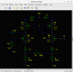
In the case of this asymmetric differential pair, what would be the suitable constraints besides max/min current range ?

See ASCO circuit optimizer

Gm2.png
 
Last edited:

There are a set of complexity levels. As far as I understand, you want to find the optimum output impedance. That does not necessarily imply that you should size the two branches exactly equal, nor that you want the DC points to be equal at the input. If all these are free, you have 13 free parameters.

* Wp1,Wp2,Lp1,Lp2,Wn1,Wn2,Ln1,Ln2,Ip,In,Vinp,Vinn,Rx

Then set the requirements

* Lmin < L < Lmax (probably given by the pdk)
* Wmin < W < Wmax (probably not given by the pdk, but area would dictate this)
* 0 < I < Imax (given by a power specification)
* 0 < Rx < Rmax (some MOhm, perhaps)
* 0 < Vin < Vdd
* 0 < Vdd < Vmax (whatever the process handles)

Etc, then the number of variables can quickly be reduced by setting the two branches equal.

ASCO can of course be used with a proper interface to the circuit simulator. If your simulator supports Monte Carlo, you can also do it inside that environment, by defining the variables as random variables within the constraints above. Sometimes, quite interesting configurations can pop out.
 

ASCO can of course be used with a proper interface to the circuit simulator. If your simulator supports Monte Carlo, you can also do it inside that environment, by defining the variables as random variables within the constraints above. Sometimes, quite interesting configurations can pop out.

See Circuit optimization with ngspice

Why do you suggest Monte Carlo ? Is it a separate optimization method since I notice that ASCO is using differential evolution algorithm ?
 

See Circuit optimization with ngspice

Why do you suggest Monte Carlo ? Is it a separate optimization method since I notice that ASCO is using differential evolution algorithm ?

I worked quite a lot with ngspice and ASCO before and found that they work OK to a certain point (in this case, should be fine for a limited set of transistors and use cases). But the problem typically explodes when you add AC, tran, noise, DC, gain, and other spec points. That's true for most optimizers, like those in cadence or MunEDA's WiCKed, etc.

(Generally, I do not like to refer to wikipedia, but yet: http://en.wikipedia.org/wiki/Monte_Carlo_method#Simulation_and_optimization)

For me, and that's my personal view, I quite often find it easier to kick off a simulation where e.g. sizes are randomly selected and keep on running sims after sims over the night/weekend and denote the results that give me better and better results. From the results, I can also tighten the constraints and iteratively improve my solutions.

It's a bit naïve and inefficent use of simulators, I admit, but still IMO quite powerful anyway.
 
Now, I am looking at monte-carlo example of ngspice. I am new to this monte-carlo circuit simulation.

I checked **broken link removed** but it does not really say much.

What does the following ngspice script do in details ? Why gaussian or uniform distribution ?

Code:
* Effecting a Monte Carlo calculation in ngspice
V1 N001 0 AC 1 DC 0
R1 N002 N001 141
*
C1 OUT 0 1e-09
L1 OUT 0 10e-06
C2 N002 0 1e-09
L2 N002 0 10e-06
L3 N003 N002 40e-06
C3 OUT N003 250e-12
*
R2 0 OUT 141
.control
  let mc_runs = 5
  let run = 0
  set curplot=new          $ create a new plot
  set scratch=$curplot     $ store its name to 'scratch'
  setplot $scratch         $ make 'scratch' the active plot 
  let bwh=unitvec(mc_runs) $ create a vector in plot 'scratch' to store bandwidth data
  
* define distributions for random numbers:
* unif: uniform distribution, deviation relativ to nominal value
* aunif: uniform distribution, deviation absolut
* gauss: Gaussian distribution, deviation relativ to nominal value
* agauss: Gaussian distribution, deviation absolut
* limit: if unif. distributed value >=0 then add +avar to nom, else -avar
  define unif(nom, rvar) (nom + (nom*rvar) * sunif(0))
  define aunif(nom, avar) (nom + avar * sunif(0))
  define gauss(nom, rvar, sig) (nom + (nom*rvar)/sig * sgauss(0))
  define agauss(nom, avar, sig) (nom + avar/sig * sgauss(0))
*  define limit(nom, avar) (nom + ((sgauss(0) ge 0) ? avar : -avar))
  define limit(nom, avar) (nom + ((sgauss(0) >= 0) ? avar : -avar))
*
*
  dowhile run < mc_runs    $ loop starts here
*
*    alter c1 = unif(1e-09, 0.1)
*    alter c1 = aunif(1e-09, 100e-12)
*    alter c1 = gauss(1e-09, 0.1, 3)
*    alter c1 = agauss(1e-09, 100e-12, 3)
*
    alter c1 = unif(1e-09, 0.1)
    alter l1 = unif(10e-06, 0.1)
    alter c2 = unif(1e-09, 0.1)
    alter l2 = unif(10e-06, 0.1)
    alter l3 = unif(40e-06, 0.1)
    alter c3 = limit(250e-12, 25e-12)
*
    ac oct 100 250K 10Meg
*	
* measure bandwidth at -10 dB
    meas ac bw trig vdb(out) val=-10 rise=1 targ vdb(out) val=-10 fall=1
* 
    set run ="$&run"            $ create a variable from the vector
    set dt = $curplot           $ store the current plot to dt
    setplot $scratch            $ make 'scratch' the active plot
    let vout{$run}={$dt}.v(out) $ store the output vector to plot 'scratch'
	let bwh[run]={$dt}.bw       $ store bw to vector bwh in plot 'scratch'
    setplot $dt                 $ go back to the previous plot
    let run = run + 1      	
  end    $ loop ends here
*  
  plot db({$scratch}.allv)
  echo
  print {$scratch}.bwh
.endc

.end
 

I do not have ngspice installed here, but as it looks:

* You have three LC tanks and two resistors in a sort of filtering function from N001 to OUT.
* Then a set of variable definitions as well as distribution definitions. The syntax is not really known to me, but the help text sort of gives a clue.
* Then five iterations are run where the tool picks a random number based on the specification you give.
* The alter will pick a new value for the parameters each time in the loop.
* Then measure the bandwidth, etc., in your case, you would have to put an ac 1-amp source and measure the max V(OUT) voltage.
* Then it's about plotting.

Gaussian or uniform is up to the user/provider to decide. The statistical distribution is given by the processing of the components. Mostly assumed to be Gaussian.

In your diff-pair approach you would use the uniform distribution between a minimum and maximum value.
 
R1 N002 N001 141
R2 0 OUT 141

I believe these two resistors are for input and output impedance. But why "141" ?

@jjx

Besides, do you publish your circuit optimization work with ASCO or ngspice monte-carlo in any public internet domain ?
 
Last edited:

No, not published as such. Nowadays, I have the luxury to have all tools paid for and can work with more or less unlimited cadence and matlab licensing.

141 - I would guess it's scaled by sqrt(2) to normalize rms to a more readable number - possibly. Other than that it does not make any other sense from an electrical point of view.
 

I am still looking at the ASCO manual.

0 < Rx < Rmax (some MOhm, perhaps)

Rx should represent ouput impedance, right ?

How am I suppose to optimize this ? I do not need all those symbolic equation variables, gm and ro of the mosfets, right ?

I only need to set up a simple output impedance measurement circuit in AC analysis with input source shorted to GND, right ?
 

Rx is the resistance you have between the two current sources in the tails.

No, you do not need any equations. Just let the simulator do the job. As you mentioned, measure the output impedance. The input should be shorted to AC ground but its DC level could also be a free parameter that you optimize.

In your simulation then note the values for which you get higher output impedance and eventually you will get the settings you are looking for.

Do not forget that you will get a numerical solution to your problem from which you might or might not be able to conclude important design guidance. To get an analytical result, you would have to solve the equations, but IMO they are inaccurate anyway, especially when you look for accurate optimization. They can give you a hint towards where to find the optimum point, but they will not reach all the way.

If you wouldn't have the feedback in one of the branches (asymmetric) the answer would analytically be much simpler and straight forward.
 
its DC level could also be a free parameter that you optimize

I am afraid in reality, I could not optimize the DC level, since this is a gyrator-based active inductor which should be able to handle wide range of input DC level

feedback in one of the branches (asymmetric)

Which circuit node is 'feedback' ?
 

I was thinking of the diode connected M4. Feedback was perhaps not the best word.
 

.PARAM TMEAS_START = '(NO_PERIODS-1)*INP_PERIOD'
.PARAM TMEAS_STOP = '(NO_PERIODS)*INP_PERIOD'
.PARAM TMEAS_1 = 'TMEAS_STOP -3*INP_PERIOD/4'
.PARAM TMEAS_2 = 'TMEAS_STOP -1*INP_PERIOD/4'

What are the purposes of these four PARAM ? They are not used in the following inv.sp ?

Besides, if I want to measure output impedance, should I fix the test current going into the output node while varying the test voltage at output node ? OR the other way round ?

Code:
*Digital inverter

.PARAM V_SUPPLY = '#V_SUPPLY#'
.PARAM INP_FREQ = '#INP_FREQ#'
.PARAM INP_PERIOD = '1/INP_FREQ'
.PARAM NO_PERIODS = '4'
.PARAM TMEAS_START = '(NO_PERIODS-1)*INP_PERIOD'
.PARAM TMEAS_STOP = '(NO_PERIODS)*INP_PERIOD'
.PARAM TMEAS_1 = 'TMEAS_STOP -3*INP_PERIOD/4'
.PARAM TMEAS_2 = 'TMEAS_STOP -1*INP_PERIOD/4'

*** *** SUPPLY VOLTAGES *** ***
VDD VDD 0 {V_SUPPLY}
VSS VSS 0 0

*** *** INPUT SIGNAL *** ***
VSIG IN VSS PULSE {V_SUPPLY} 0 'INP_PERIOD/2' 'INP_PERIOD/1000'
+               'INP_PERIOD/1000' 'INP_PERIOD/2' 'INP_PERIOD'

*** *** ROUT TEST CIRCUIT *** ***
MP OUT IN VDD VDD P1 W='#WP#'   L=#LMIN# 
MN OUT IN VSS VSS N1 W='#WP#/2' L=#LMIN# 

CL OUT VSS 3p

*** *** ANALYSIS *** ***
.TRAN 'INP_PERIOD/1000' 'NO_PERIODS*INP_PERIOD'
*
*.PROBE TRAN V(IN)
*.PROBE TRAN V(OUT)
.OPTION POST PROBE ACCURATE
.include modelcard.nmos
.include modelcard.pmos
.END
 

Those parameters are just used to setup the measurements related to a clock frequency. This enables a more flexible way of sweeping/parameterizing the simulator. And, no, they are not used, so probably left-overs from some old settings.

For your test fix a 1-A AC current and measure the AC voltage.

The DC output voltage you could either observe and discard tests with wrong DC. Or set through a passive network. There is a thread on this currently on-going in this forum (as you know...).

https://www.edaboard.com/showthread.php?377214-Noise-in-CMOS-Inverter
 
This is my inv.sp file.

When I look into the extract/ directory, I saw few measurement files such as P_SUPPLY, VHIGH and VLOW

I still think if I want optimum output impedance, I cannot sacrifice Vih or Vil even though I am using this CMOS inverter mostly in its transition region (in analog circuit rather than in digital circuit)

What do you guys think ?

Code:
*CMOS inverter 

.PARAM V_SUPPLY = '#V_SUPPLY#'
.PARAM V_OUT = '#V_OUT#'
.PARAM INP_FREQ = '#INP_FREQ#'
.PARAM INP_PERIOD = '1/INP_FREQ'
.PARAM AC_POINTS = 10000
.PARAM AC_START = 10
.PARAM AC_STOP = 1000000

*** *** SUPPLY VOLTAGES *** ***
VDD VDD 0 {V_SUPPLY}
VSS VSS 0 0

*** *** INPUT SIGNAL *** ***
VSIG IN VSS VSS

*** *** CIRCUIT UNDER TEST *** ***
MP OUT IN VDD VDD P1 W='#WP#'   L=#LMIN# 
MN OUT IN VSS VSS N1 W='#WP#/2' L=#LMIN# 

CL OUT VSS 3p

*** *** ROUT TEST SIGNAL *** ***
VOUT VOUT '#V_OUT#' VSS
IOUT OUT VOUT 1A

*** *** ANALYSIS *** ***
.AC dec 'AC_POINTS' 'AC_START' 'AC_STOP'
*
*.PROBE TRAN V(IN)
*.PROBE TRAN V(OUT)
.OPTION POST PROBE ACCURATE
.include modelcard.nmos
.include modelcard.pmos
.END
 

@jjx

I am facing the following ASCO error for View attachment inv.zip. I have already had ROUT objective in inv.cfg. What else did I miss ? [

inv.cfg

Code:
#Optimization Flow#
Alter:yes           $do we want to do corner analysis?
MonteCarlo:no       $do we want to do MonteCarlo analysis?
AlterMC cost:3.00   $point at which we want to start ALTER and/or MONTECARLO
ExecuteRF:no        $execute or not the RF module to add RF parasitics?
SomethingElse:      $
#


#DE#
choice of method:3
maximum no. of iterations:50
Output refresh cycle:2
No. of parents NP:10
Constant F:0.5
Crossover factor CR:1
Seed for pseudo random number generator:3
Minimum Cost Variance:1e-6
Cost objectives:10
Cost constraints:10000
#


# ALTER #
.control 
alter vdd=[2.0 2.1 2.2]
run
.endc
*.protect
*.inc [../models/cmos035_slow.mod ../models/cmos035_typ.mod ../models/cmos035_fast.mod]
*.unprotect
*.temp [-40 +25 +85]
*.param
*+    V_SUPPLY=[2.0 2.1 2.2]
*.protect                                                $ As much as 6 variables can be swept at the same time.
*.lib hl49ciat57k5r200.mod [mos_wcs mos_nom mos_bcs]     $ Format is [a] or [a b] or ... [a b c d e f] =>1 space
*.unprotect                                              $ and not :[ a], [a ], [ a ] => space is not really necessary
*.temp [-40 +25 +85]                                     $ and not :[a  b]            => only 1 ' ' between 'a' and 'b'
*.param                                                  $ Add '*' to skip a line
*+    vddd=[2.25 2.50 3.30]                              $
*+    kc=[0.95 1.05]:LIN:10        $ LIN not yet implemented
*+    kr=[0.87 1.13]:LOG:10        $ LOG not yet implemented
*+    Ierror=[0.7 1.3]
*+    k00=[0 1]
*+    k01=[0 1]
*+    k02=[0 1]
*+    k03=[0 1]
*+    k04=[0 1]
*+    k05=[0 1]
*+    k06=[0 1]
*+    k07=[0 1]
*+    k08=[0 1]
*+    k09=[0 1]
#


#Monte Carlo#
NMOS_AVT:12.4mV           $ This values will be divided by sqrt(2) by the program
NMOS_ABETA:7.3%           $ 'm' parameter is taken into account
PMOS_AVT:10.9mV           $
PMOS_ABETA:3.7%           $
SMALL_LENGTH:0.0u         $ Small transistors if l<= SMALL_LENGTH
SMALL_NMOS_AVT:20mV       $ Small transistors parameters
SMALL_NMOS_ABETA:10%      $
SMALL_PMOS_AVT:10mV       $
SMALL_PMOS_ABETA:5%       $
R_DELTA:0.333%            $ Resistors matching at 1 sigma between two resistors
L_DELTA:0.333%            $ Inductors matching at 1 sigma between two inductors
C_DELTA:0.333%            $ Capacitors matching at 1 sigma between two capacitors
#


# Parameters #
Supply voltage:#V_SUPPLY#:2.0:0:0:LIN_DOUBLE:---
Temperature:#TEMP#:25:0:0:LIN_DOUBLE:---
Minimal gate length:#LMIN#:0.35u:0:0:LIN_DOUBLE:---
Input frequency:#INP_FREQ#:850E6:0:0:LIN_DOUBLE:---
PMOS width:#WP#:10000u:1m:10m:LIN_DOUBLE:OPT
Output voltage:#V_OUT#:1:1:5:LIN_DOUBLE:OPT
#


# Measurements #
#P_SUPPLY:---:MIN:0
#VHIGH:OUT:GE:1.95
#VLOW:OUT:LE:0.05
ROUT:OUT:GE:1000
#


# Post Processing #
#


#this is the last line

inv.sp

Code:
*CMOS inverter 

.PARAM V_SUPPLY = '#V_SUPPLY#'
.PARAM V_OUT = '#V_OUT#'
.PARAM INP_FREQ = '#INP_FREQ#'
.PARAM INP_PERIOD = '1/INP_FREQ'
.PARAM NO_PERIODS = '4'
.PARAM TMEAS_START = '(NO_PERIODS-1)*INP_PERIOD'
.PARAM TMEAS_STOP = '(NO_PERIODS)*INP_PERIOD'
.PARAM AC_POINTS = 10000
.PARAM AC_START = 10
.PARAM AC_STOP = 1000000

*** *** SUPPLY VOLTAGES *** ***
VDD VDD 0 {V_SUPPLY}
VSS VSS 0 0

*** *** INPUT SIGNAL *** ***
VSIG IN VSS VSS

*** *** CIRCUIT UNDER TEST *** ***
MP OUT IN VDD VDD P1 W='#WP#'   L=#LMIN# 
MN OUT IN VSS VSS N1 W='#WP#/2' L=#LMIN# 

Lf OUT IN 0.01
** The input can be either biased with a DC source, or a DC feedback circuit. Using a DC feedback circuit (RC, inductor, whatsoever) makes only sense if there's no DC voltage source, see https://www.edaboard.com/showthread.php?377214-Noise-in-CMOS-Inverter&p=1617292&viewfull=1#post1617292  


*** *** ROUT TEST SIGNAL WITH FIXED 1A CURRENT AND VARIABLE TEST VOLTAGE (VOUT) *** ***
VOUT OUT '#V_OUT#' VSS
IOUT OUT VOUT 1

*** *** ANALYSIS *** ***
.AC dec 'AC_POINTS' 'AC_START' 'AC_STOP'
*
*.PROBE TRAN V(IN)
*.PROBE TRAN V(OUT)
.OPTION POST PROBE ACCURATE
.include modelcard.nmos
.include modelcard.pmos
.END

ROUT

Code:
# Info #
Name:ROUT
Symbol:Z_ROUT
Unit:Ω
Analysis type:AC
Definition:Output Impedance
Note:
#

# Commands #
.measure ac #SYMBOL# par('VOUT/1')
#

[phung@archlinux inv]$ ls -al
total 112
drwxr-xr-x 3 phung phung 4096 Jun 23 15:33 .
drwxr-xr-x 4 phung phung 4096 Jun 15 00:41 ..
-rw-r--r-- 1 phung phung 56287 Jun 23 15:34 archlinux.log
-rw-r--r-- 1 phung phung 269 Jun 23 15:34 archlinux.out
-rw-r--r-- 1 phung phung 796 Jun 23 15:34 archlinux.sp
-rw-r--r-- 1 phung phung 861 Jun 23 15:34 archlinux.tmp
-rw-r--r-- 1 phung phung 285 Jun 23 15:34 asco.log
drwxr-xr-x 2 phung phung 4096 Jun 23 15:30 extract
-rw-r--r-- 1 phung phung 2822 Jun 23 15:32 inv.cfg
-rw-r--r-- 1 phung phung 292 May 2 00:21 inv.net
-rw-r--r-- 1 phung phung 1185 Jun 23 15:33 inv.sp
-rw-r--r-- 1 phung phung 6528 Feb 16 2017 modelcard.nmos
-rw-r--r-- 1 phung phung 6530 Feb 16 2017 modelcard.pmos
[phung@archlinux inv]$
[phung@archlinux inv]$ asco -ngspice inv.sp

ASCO-0.4.10 - Copyright (c) 1999-2016 Joao Ramos
This program is distributed in the hope that it will be useful,
but WITHOUT ANY WARRANTY; without even the implied warranty of
MERCHANTABILITY or FITNESS FOR A PARTICULAR PURPOSE. See the
GNU General Public License for more details.

INFO: ngspice initialization on 'archlinux'
INFO: Initialization has finished without errors on 'archlinux'
INFO: Current directory on 'archlinux': /home/phung/Documents/Grive/Personal/Analog/Active_Inductor/frequency_trap/optimization/inv

PRESS CTRL-C TO ABORT

INFO: Starting global optimizer on 'archlinux'...
INFO: errfunc.c - CostFunction -- Cost is very close to zero. This can either be (a) due to an error or because (b) there is not an objective in category # Measurements # in the *.cfg file.
INFO: errfunc.c - Step7 -- altermc=2
INFO: errfunc.c - CostFunction -- Cost is very close to zero. This can either be (a) due to an error or because (b) there is not an objective in category # Measurements # in the *.cfg file.


INFO: de36.c - Ctrl-C key pressed.
INFO: Ending optimization


INFO: Starting local optimizer on 'archlinux'...
INFO: ASCO has ended on 'archlinux'.
[phung@archlinux inv]$
 

Ok, as I do not have ASCO installed here I am not really able to judge. However, it seems like the cost function is not that well defined. What is your cost measure?
 

I have solved the ngspice running error. However, from archlinux.out and summary.txt , I found that ROUT is not measured at all.

I have also modified the ALTER section within inv.cfg accordingly, however ROUT is still not being measured and optimized.

Could you describe what the following command do since par() is not documented in the manual as well as the other tutorial example code ?

.measure tran #SYMBOL# rms par('i(vdd)*v_supply') from='tmeas_start' to='tmeas_stop'

I suspect that my low AC output impedance after optimization could be due to incorrect usage of this .measure command

Could you suggest if this is the case ?

I have attached all the updated , asco related inv files here View attachment inv.zip
 

Status
Not open for further replies.

Similar threads

Part and Inventory Search

Welcome to EDABoard.com

Sponsor

Back
Top