loki3118
Junior Member level 2

Thank you everyone for you help with my earlier post regarding a half bridge amplifier. I got that simulation to work beautifully.
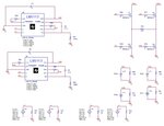
My next task is to model a full bridge amplifier. This design is giving me a lot more trouble than the previous iteration. No matter what recommendations that the online resources suggest I cannot get the circuit to converge. I'm at the point that there must be something completely wrong with my circuit design. I've looked for something obviously wrong with the circuit but I believe that I am too close to see the error.
Does anyone see something obviously wrong with the circuit? Also does anyone have any suggestions that I could try to get it to converge?
Thank you for your help!

