Continue to Site

Welcome to EDAboard.com

Welcome to our site! EDAboard.com is an international Electronics Discussion Forum focused on EDA software, circuits, schematics, books, theory, papers, asic, pld, 8051, DSP, Network, RF, Analog Design, PCB, Service Manuals... and a whole lot more! To participate you need to register. Registration is free. Click here to register now.

OrCAD Allegro PCB Editor Footprint do not match Capture part symbol

Status
Not open for further replies.

FredCailloux

Junior Member level 1
Joined
Feb 14, 2017
Messages
19
Helped
5
Reputation
10
Reaction score
4
Trophy points
3
Location
In Quebec
Activity points
274
OrCAD16.6 - In Capture using 3 MOSFET assigned footprint TO3
(standard in \pcb_lib\symbols\ TO3.dra). When jumping to Allegro PCB Editor trying to use the QuickPlace tool, all my schematic parts are placed on top corner except the 3 MOSFET TO3.
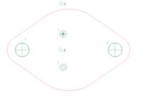

Issued error "Pin number do not match between symbol and component".
This is because the TO3.dra include 4 pins, pin 3 and 4 are the same TO3 casing, yet the MOSFET only has 3 pins named 1 2 and 3. On the footprint the TO3 end holes are marked like two separate pin 3 and 4. Yet, electrically speaking they are identical. Allegro PCB Editor expect only 3 pins from the symbol, yet there are 4 pins on the footprint. Hence, the error.

I want to avoid having to modify the MOSFET Capture Symbol with an extra pin just to match the TO3.dra footprint. It would not be representative of the electrical identity with MOSFET.

How can I correct this problem at the footprint level?
How can I make the footprint pins 3 and 4 the same pin?

Thank you for your help
 

Not sure why the schematic and Pcb symbols don't match, but personally I'd make the schematic symbol have four pins. I totally disagree with your comment that "it would not be representative of the electrical identity...". There are TWO physical points (mtg holes) where you can connect to the drain (or whatever signal the case is), just because they're electrically identical doesn't mean they don't exist. Would you object to a DIP package that had multiple GROUND pins?

When it comes to actually routing to the two mtg holes, how will that work if one doesn't exist?
 
Practically speaking, I agree 100% with you. The quickest solution is to modify the Capture Symbol. This is what I will end-up doing anyway. But on a more educational point of view, I cannot believe that such a basic situation has not been taken into consideration by OrCAD programmers. Yes, the solution is functional and practical, but it is not logical. A transistor has only one collector. That practical solution would imply that if I change the configuration of the transistor from a TO3 to a TO220 I would have to literally change the Symbol in the schematic rather then just changing it's attributed footprint.

So then, how can I modify the footprint ? Can I, for instance, simply eliminate the pin 4 on the footprint?
Or, is there a way to tell the PCB editor that pin 3 and pin 4 are the same and force a copper trace between the two? Thank for your help
 

With a state-of-the-art layout tool, you can map a transistor symbol to different footprints, lets say a MOSFET either to a 3-pin SOT-23 or a 8-pin SO8, using different component definitions in the part library. In the latter case, the single drain symbol pin shows 5 pin numbers.

But I don't know if it's possible with Allegro, I remember there have been restrictions in their library scheme. An Allegro user should tell.
 

That practical solution would imply that if I change the configuration of the transistor from a TO3 to a TO220 I would have to literally cbhange the Symbol in the schematic rather then just changing it's attributed footprint.
You can have a component in different packages with different pin outs. For example, a MOSFET in one package may map pin 1 to Drain, pin 2 to Source and pin 3 to Gate, yet the same device in a different package may map pin 3 to Drain, etc. You better hope your schematic reflects this, or your in for a heap of aggravation when you try to debug.
 

Status
Not open for further replies.

Part and Inventory Search

Welcome to EDABoard.com

Sponsor

Back
Top