Continue to Site

Welcome to EDAboard.com

Welcome to our site! EDAboard.com is an international Electronics Discussion Forum focused on EDA software, circuits, schematics, books, theory, papers, asic, pld, 8051, DSP, Network, RF, Analog Design, PCB, Service Manuals... and a whole lot more! To participate you need to register. Registration is free. Click here to register now.

Opamp photodiode analysis...

Status
Not open for further replies.

adinogcas

Junior Member level 1
Joined
Jan 28, 2010
Messages
17
Helped
1
Reputation
2
Reaction score
0
Trophy points
1,281
Activity points
1,424
Hello all,

I have confusion when analyzing this simple basic circuit:

I have a circuit that amplify the signal from a photodiode (D1) with a opamp U1 and R1. Here is my calculation for Vo: (suppose ideal opamp)

When there is light, D1 creates current Id, whose direction goes from D1 to Vn (cant go to opamp) and goes to Vo. So I have:

Vn-Vo=R1*Id;
Vn=Vp=0 (virtual ground)

=>Vo= -R1*Id

That's my result!!! So why in the book, it says Vo=R1*Id (not inverting) ? If Vo=R1*Id, there is a current will flow from Vo to Vn to cancel Id???
 

In your circuit the photo-diode does not have a reverse bias voltage so it behaves as a tiny solar-cell. I think light will cause the output of the opamp to go negative.
The current in the photo-diode is the same as the current in R1.
 

Actually, the circuit has a positive output voltage. For a vivid explanation, I suggest two different ways:
- assume zero current flow at the beginning. Then the photo current will build up a photoelement voltage, negative at the
cathode. The OP gain causes a positive voltage at the output.
- consider, that the photocurrent is a reverse current. Only a positive output voltage can cause a reverse current through
R1 and D1.

To anticipate a possible question. Yes, the photocrrent has the same direction in all photo diode operation modes.
But in photoelement mode, the photo current is cancelled by a forward current, if no external load exists.

I notice that this basic circuit often causes confusion. It has been discussed repeatedly at edaboard, see e.g.:
 

So the book was wrong!!! The confusion here is the direction of current. I was confused.

Ok, so I have 1 more analysis for opmap. V1, V2 are inputs. Assume ideal opamp, and here is my calculation:

(Vo-Vn)/R1 = (Vn-V1)/R2 <-----Here is the confusion part, what should it be Vn-V1 or V1-Vn?

So what is the direction of current flows from V1? Will it be from (V1->Vn->Vo) or (Vo->Vn->V1) or (V1->Vn, Vo->Vn).

Next question is:
if direction is V1->Vn->Vo, how do I know that V1>Vn so current will flow in that direction. Same question for other direction...
 

So what is the direction of current flows from V1? Will it be from (V1->Vn->Vo) or (Vo->Vn->V1) or (V1->Vn, Vo->Vn).
Clearly no current flows into Vn for an ideal OP. So (V1->Vn->Vo) or (Vo->Vn->V1) are both correct, depending on the input voltage polarity.

So the book was wrong!
I don't know. Id polarity isn't shown in the schematic. But the the absolute output
voltage is positive, when the photo diode is illuminated.

If Id designates the (reverse) photo current, Vo=R1*Id is correct.
 

I think I have an answer for the PD problem. As circuit shows: Vn=Vp=0, which creates zero voltage across the D1 (and always be, because of the opamp). Which means PD is in reversed bias, or in photo conducting mode. Therefore, when a light strike the PD, it will create photocurrent (Id) flows from cathode(N-type) to anode(P-type). The formula will be:

Vo-Vn=R1*Id
Vn=Vp=0
=> Vo=R1*Id !!! (the book is right!!! and I was wrong :D)

If my though is wrong, please correct! Thanks
 

OK, so now I have phototransistor (PT) instead of photodiode (PD)...Can anyone tell me if this circuit is wrong?

Here is my analysis, when a light strikes PT, it will create a Photo current from collector to emitter. Direction of current should be Vo->Vn->V1

(Vo-Vref)/R1 = (Vref-V1)/R2
<=>Vo = R1/R2*Vref - R1/R2*V1 + Vref
<=>Vo = 5.7*Vref - 4.7*V1

Which mean the output will be 5 times the input and is inverted. Also it oscillates at 5.7*Vref (V). Am I right? Can PT be used in this way, like PD?
 

The circuit is (partly) working, but the description isn't correct. Basically, a phototransistor is a current rather than
a voltage source. R2 could be omitted without changing the basic operation, a small series resistor may be possibly
required to achieve stability, a capacitor in parallel to R1 can do the same. The output has it's bias level at Vref rather
than 5.7 * Vref.

The circuit operation can be described best by this equation:

Vo = Ic*R1 + Vref
 

What do you mean by "partly working"? My purpose is to detect the intensity of a light.

So I should take out R2 and replace R1 to 5k to have the gain of 5 of the photo current? And if I put Vref=0, it should be exactly as the circuit above (Photodiode circuit)?

1 more question. I have seen this kind of circuit but with the power supply connect to R then connect to PT (Vs->R->PT). So what is a difference ?
 

Just quick question...


What is the output of this circuit? (suppose Vdac=0=GND)
Ip=Current Photo

will it be Vo= -Ip * R
or Ip*R?

And why? Because someone told me it should be -Ip*R not Ip*R. And most of transimpedance circuit use in different configuration.

I am getting confused here. Please help!
 

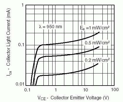
I don't see a reasonable purpose of the circuit. A phototransistor doesn't generate a photocurrent Ip at Vce = 0. So you get effectively
not output with VDAC = 0.

The equation given with above circuit is correct as well, but with the reservation, that a minimum Vref respectively VDAC of
0.1...0.3 V is required to generate a photocurrent.

Vo = Ic*R1 + Vref

See a the Vce/Ice charateristic from a phototransistor datasheet:

90_1267269924.gif
 

    adinogcas

    Points: 2
    Helpful Answer Positive Rating
Status
Not open for further replies.

Similar threads

Part and Inventory Search

Welcome to EDABoard.com

Sponsor

Back
Top