Continue to Site

Welcome to EDAboard.com

Welcome to our site! EDAboard.com is an international Electronics Discussion Forum focused on EDA software, circuits, schematics, books, theory, papers, asic, pld, 8051, DSP, Network, RF, Analog Design, PCB, Service Manuals... and a whole lot more! To participate you need to register. Registration is free. Click here to register now.

OP-Amp Feedback Loop Layout

Status
Not open for further replies.

juz_ad

Full Member level 2
Full Member level 2
Joined
Dec 17, 2011
Messages
130
Helped
0
Reputation
0
Reaction score
0
Trophy points
1,296
Activity points
2,541
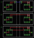
I have a PCB design that uses 2x different boards with an inter-board connector between them. I've realised that I might have done something stupid with the trace/layout that one of the connectors is using - hopefully the pic should explain it...
Screen Shot 2016-10-06 at 18.38.22.png

v1) PCB 1 has an op-amp buffer, the output goes to an inter-board connector which then goes to the input of an inverting op-amp config on PCB 2.

v2) Am I right that - as far as the circuit/layout is concerned - that buffer feedback loop essentially runs all the way to the input of the op-amp on the 2nd PCB and back again?

v3) How do I stop that? Would putting a R right at the buffer output and then, if necessary, compensating with an R in the gain of the next, inverting op-amp?

Would that put the buffer feedback loop only on PCB 1? Hope that's clear/makes sense.

Thanks in advance.

/ J
 

Hi,

Not sure, if you put the feedback resistor on the same board as the buffer, I'd have thought that the feedback loop wouldn't need to be prolonged into the second board, I don't understand much but that wouldn't make any sense (even) to me regarding keeping traces as short as possible.

Do not know the answer to the second part of the question about compensating with r in gain of next.
 

The second schematic doesn't make sense as shown, it misses a connector for the feedback path.

To understand if the loop layout has any relevance for the amplifier performance, some basic parameters must be known like:
- amplifier and signal bandwidth
- resistor values

I guess, each topology can be useful under specific circumstances.
 

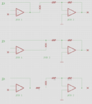
Thanks for the replies - I don't think I've explained this clearly (or maybe I'm imagining the problem...) - I'll try again.

Screen Shot 2016-10-07 at 13.44.34.png

1) This represents the physical layout. A buffer output on PCB1 connected to an inverting op-amp input on PCB2 via an inter-board connector (the blue trace)

2) Is what the circuit 'sees' - a long trace from the output of the buffer to the input of the inverting op-amp

3) This is what I'm worried about - as far as the circuit is concerned - it's not a single trace from output to input via a connector - it's also a long, extended feedback path/loop that travels all the way from PCB1 to PCB2 and back again.

That strikes me as not a very good PCB layout decision.

Is that a correct assessment in regards to the actual circuit rather than the physical layout?

So - my questions is - if this is correct and is potentially a problem - how do I solve it. How do I constrain the feedback path to the shortest possible area and ensure that only a single trace is travelling between boards - not a whole feedback loop.

My suggestion was to put a resist at the output of the buffer.

Thanks,

/ J
 

Status
Not open for further replies.

Part and Inventory Search

Welcome to EDABoard.com

Sponsor

Back
Top