Continue to Site

Welcome to EDAboard.com

Welcome to our site! EDAboard.com is an international Electronics Discussion Forum focused on EDA software, circuits, schematics, books, theory, papers, asic, pld, 8051, DSP, Network, RF, Analog Design, PCB, Service Manuals... and a whole lot more! To participate you need to register. Registration is free. Click here to register now.

op-amp based bandgap reference problem

Status
Not open for further replies.

anhnha

Full Member level 6
Full Member level 6
Joined
Mar 8, 2012
Messages
322
Helped
4
Reputation
8
Reaction score
4
Trophy points
1,298
Activity points
3,684
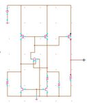
I am designing an op-amp based bandgap reference and getting this problem.

**broken link removed**
As Vdd increases, the output of op-amp also increases but at a much higher rate=> Vsg of M11, M12 decrease and the currents flowing through these transistors decrease=> bandgap voltage decreases.

Could anyone tell me how to solve this?
 

Are You sure about proper feedback? Remember that M12 works as another inverting stage. At dc simulation everything works?
 
  • Like
Reactions: anhnha

    anhnha

    Points: 2
    Helpful Answer Positive Rating
Might cut the problem into two pieces by replacing the op amp
with a vcvs of suitable gain; a low quality op amp might just
be showing you the cost of poor PSRR (or, you operating it
at points where its PSRR gets weak).
 
  • Like
Reactions: anhnha

    anhnha

    Points: 2
    Helpful Answer Positive Rating
As Vdd increases, the output of op-amp also increases but at a much higher rate=> Vsg of M11, M12 decrease and the currents flowing through these transistors decrease=> bandgap voltage decreases.

Could anyone tell me how to solve this?

As correctly pointed by Dominik
Is the op-amp connection right? I think you should interchange + and - terminals .... In a band gap the negative feed back loop has to be stronger than the positive feedback loop. The PMOS M11 and 12 provides an additional 180 phase shift. Please check the following docs

https://www.scientificbulletin.upb.ro/rev_docs_arhiva/full7771.pdf
https://web.mit.edu/magic/Public/papers/01692649.pdf

Hope this helps .... :)
 
  • Like
Reactions: anhnha

    anhnha

    Points: 2
    Helpful Answer Positive Rating
Thank you everyone.

I just check my op-amp connection and it is right. The bandgap is good for input voltage from 2 to 2.9V. However, from 2.9 to 4V, the reference voltage decreases sharply.

attachment.php


- - - Updated - - -

I just tried a vcvs with gain =140000 =103dB that is much higher than my opamp (78dB) but the output voltage curve is still similar to the one above, no improvements.

=> Not opamp problem here.

attachment.php


- - - Updated - - -

Here are the curves of I1, I2, I3 as Vin (supply voltage) increases from 2 to 4V. As you can see I1 and I2 are 100% equal.

attachment.php
 

Attachments

  • Bandgap Line regulation test.png
    Bandgap Line regulation test.png
    6 KB · Views: 454
  • I1.I2.I3.png
    I1.I2.I3.png
    14.9 KB · Views: 401
  • Bandgap_test.JPG
    Bandgap_test.JPG
    18.3 KB · Views: 391
Last edited:

Hi anhnha,

If you have done the opamp connections correctly .. can you check whether it is a start up issue or not. In a bandgap there are two stable operating points. zero voltage and the other is the required voltage. A band gap starts up by finally falls down because of start up issues. You can check the following paper but you will find a lot of other materials over net you can check them as well.

http://pe.org.pl/articles/2012/4a/67.pdf

Hope this helps .... :)
 
  • Like
Reactions: anhnha

    anhnha

    Points: 2
    Helpful Answer Positive Rating
Thank you, SIDDHARTHA HAZRA.

I don't think that is startup issue. If there is a startup prolem then the bandgap voltage should be very small (around 0V)? But as in the simulation image, as Vin increases from 2 to 4V, bandgap voltage decreases from 805mV to 799mV. That is not close to zero.
 

Hi.
Now I need to check the stability of this bandgap using stb analysis in Cadence.
I will insert iprobe in analogLib. However, could you tell me where should I break the loop and insert iprobe?
Also, do I need a startup for this bandgap?


**broken link removed**
 

As already mentioned:
The design is incomplete without details of characteristics of FETs & R values.
We have no chance to check your design. Also BJT areas are important.
 

Hi,
I used nmos2v and pmos2v in tsmc18rf.
R2 = R3 = 2.03M
R1 = 400K
R4 = 1.75M
Area:
Q1 = 4. 10^(-12) mulitpliter = 1
Q2 = 4. 10^(-12) mulitpliter = 32
 

Hi.
In some design, I see that there is a capacitor connected between the VDD and the gate of M11. Could you explain about the function of this capacitor?
 

The capacitor is for high frequency PSRR, when the loop looses its capability to correct for the disturbance and of no help at DC.

But FvM, just curious, why the BJT char is required, it approx always sees close to VBE always so couldn't fully understand why BJT char is required. But I accept we need to know the char of the PMOSes..
 
  • Like
Reactions: anhnha

    anhnha

    Points: 2
    Helpful Answer Positive Rating
Status
Not open for further replies.

Part and Inventory Search

Welcome to EDABoard.com

Sponsor

Back
Top