Continue to Site

Welcome to EDAboard.com

Welcome to our site! EDAboard.com is an international Electronics Discussion Forum focused on EDA software, circuits, schematics, books, theory, papers, asic, pld, 8051, DSP, Network, RF, Analog Design, PCB, Service Manuals... and a whole lot more! To participate you need to register. Registration is free. Click here to register now.

[SOLVED] Offsets in inverting and clamp amplifier circuit

Status
Not open for further replies.

d123

Advanced Member level 5
Joined
Jun 7, 2015
Messages
2,505
Helped
494
Reputation
992
Reaction score
525
Trophy points
1,393
Location
Spain
Activity points
27,148
Hi,

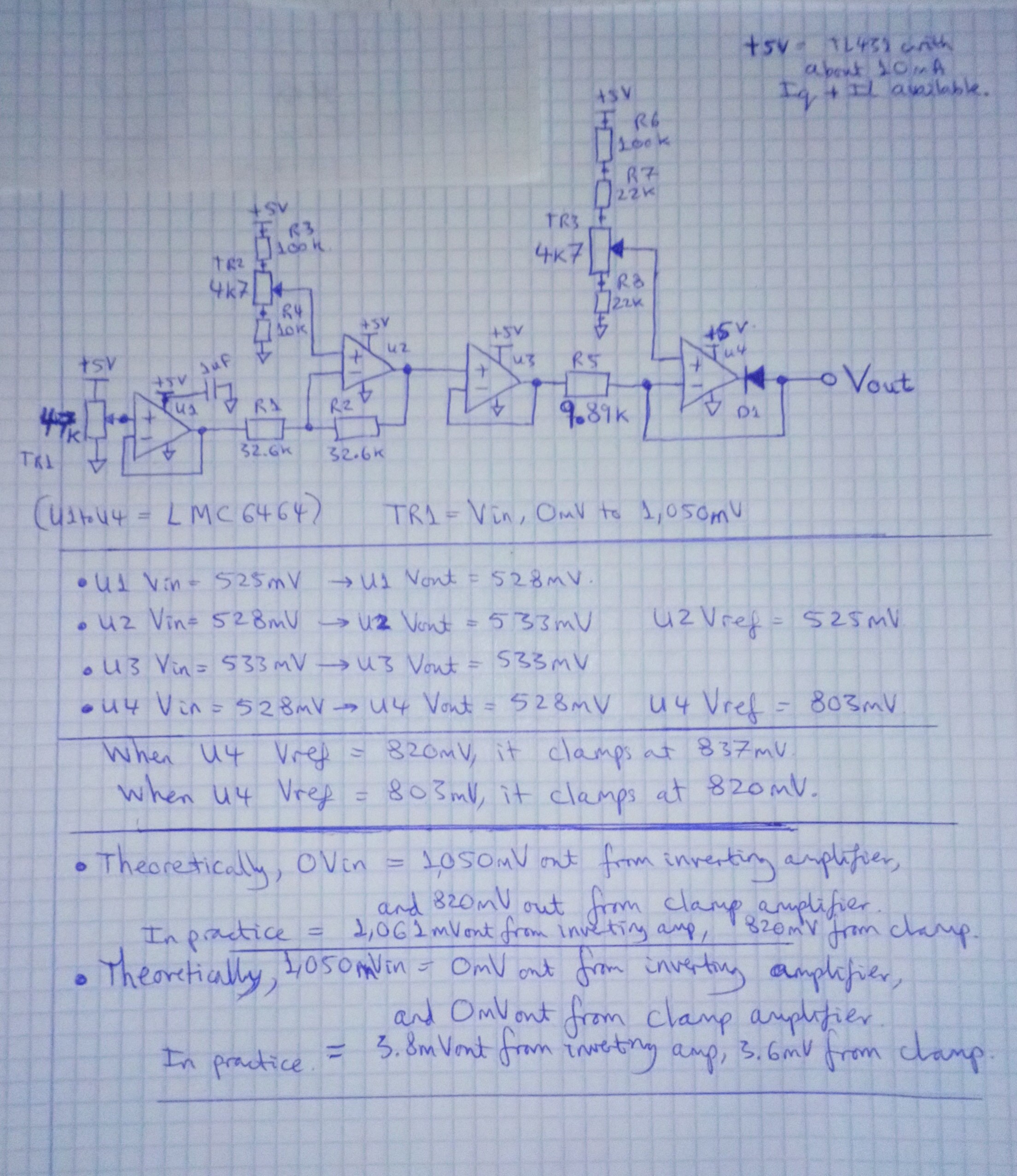
Inverting amplifier on a single supply, Vref = 525mV, 0V in = 1.050V out and 1.050V in = 0V out.
Clamp amplifier should output a clamp voltage of 820mV when its Vin goes over 820mV.
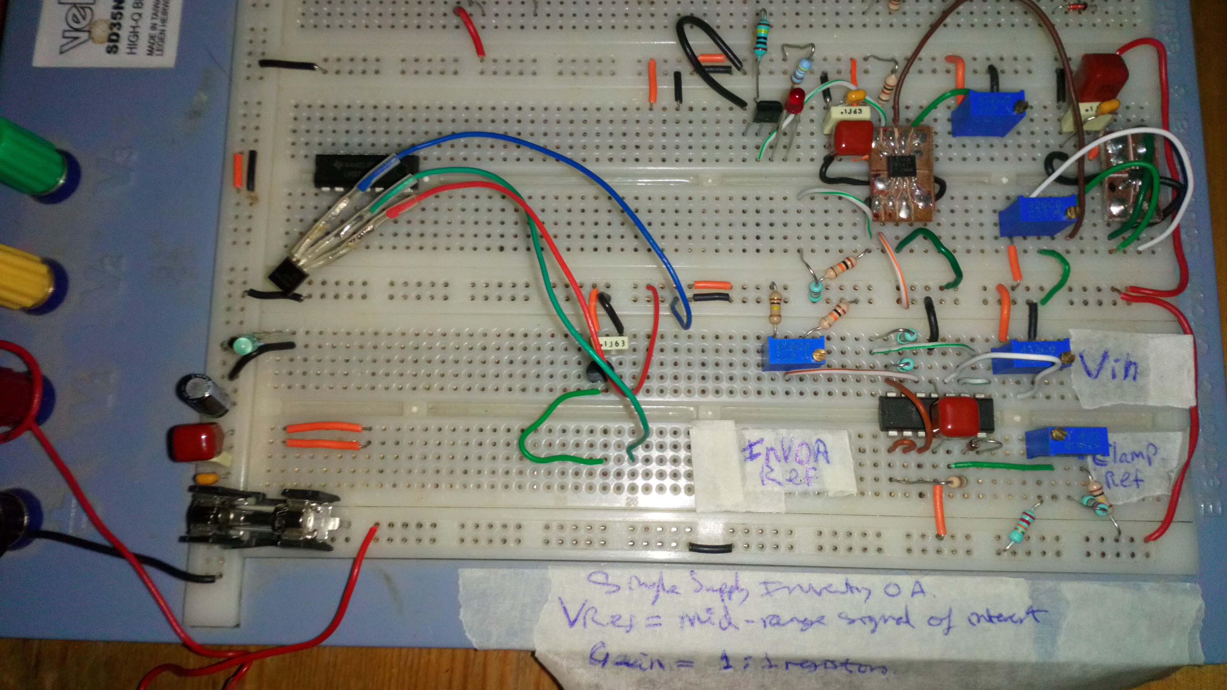
There is a buffer into a comparator (LM193) that should trigger at 850mV, not shown or connected to circuit in schematic as irrelevant to questions, also in the circuit, visible in photo. Also visible are two LM35s, not connected either.
As LM35 is +-2% inaccurate, wanted rest of circuit to be as accurate as possible to compensate for this issue.

I measured 14 points on the inverting amplifier's range from 0 Vin to 1.050 Vin and it is always an accurate ouput (compared to calculator results) with the ~8mV offset, except at 1.050 Vin = 0 Vout (1 to 3mV). DMM is supposedly +-0.8% accurate.

U1 3mV offset at its output is Vos, right?

U2 5mV offset at its output is 2*Vos, is it?

Why does U4 reference voltage need to be 803mV for clamp voltage to actually be 820mV?

This circuit is supposed to be precise, for learning purposes, at least on a breadboard at room temperature...How can I remove these offsets?

Extra question: I seem to use a lot of voltage followers, LM224 or LM324 would be acceptable in this circuit as the buffers as long as their Vin and Vout do not approach Vsupply - 1.5V and offsets are easily calibrated out?
_20201017_213539.JPG


DSC_0021.JPG


Thanks.
 

Hi,

I have lowered the inverting amplifier reference by 1 mV to get correct ouput from the clamp OA of Vout = (-Vin * (R2/R1)) + ((R1+R2/R1) * Vref).

I had a ground rail issue of different ground voltages between breadboard ground rails affecting the comparator reference level and comparator trigger level, corrected it by moving all parts onto same rails.

On the op amp clamp, I have measured from Vin- to Out, Vin+ to Out, Vin + to Vin-, did whatever calculations I could think of and I see no correlation between the clamp reference needing to be 803mV to get 820mV out when it is clamping. Any hints as to the reason?

Thanks.
 

Hi,

I have measured from Vin- to Out, Vin+ to Out, Vin + to Vin-,
These are high ohmic sesitive nodes. Just connecting a DVM to these nodes may easily shift the output by several millivolts.
Thus I´d call measurements on theese nodes as very critical.

Klaus
 
  • Like
Reactions: d123

    d123

    Points: 2
    Helpful Answer Positive Rating
Hi Klaus,

Thanks.

Hi,


These are high ohmic sesitive nodes. Just connecting a DVM to these nodes may easily shift the output by several millivolts.
Thus I´d call measurements on theese nodes as very critical.

Klaus


Would buffering the DVM probes with voltage followers be at all helpful, then?
 

Hi,

generally yes, but they will include new offset errors - be sure to keep them low.

****
You just learned how to keep offset errors low by using "the same" rail of the breadboard.
This comes close to a "star point" wiring. but even this "star point" is not "infinitely small" - as it should ideally be.

Thus my recommendation:
* Use one GND rail for the supplies ... with expectable GND currents.
* But use another rail just as reference_GND_signal without current (in best case). At this node all millivolts_critical GNDs should be joined.
For sure you need to connect both rails somewhere. - usually not that critical.

Klaus
 
  • Like
Reactions: d123

    d123

    Points: 2
    Helpful Answer Positive Rating
Hi Klaus,

I followed your advice: references on one breadboard rail, ICs on another. It cured clamp ref error.

Still couldn't understand why inverting amp reference had to be ~5mV over correct value for correct Vout at clamp In- (output). In+ high impedance, In- not so high impedance - i.e what you said about high ohmic, sensitive nodes, thanks. Used buffer between DMM positive probe and measurement points to measure again and all errors have disappeared, hooray.

I used an LM324 as the buffer, three showed 0mV offset at output with 1.000V in, one had 2mV, so used one that appears to have no offset at output.

Didn't know (for buffer) op amp non-inverting inputs don't like 5M trimpots, 4k7 and 10k work well but 5M set to 1.000V caused outputs of about 2.something volts. That mystery will have to be for another day.

Had to change comparator pull-up from 1k to 10k as it was pulling supply down from 5V to ~4.7 when triggered.

Thanks, circuit cleaned up a lot, great advice.
 

Hi
No mystery with 5M pot. The
LM324 has 45nA input bias current. Multiply it with 1.25M worst case pot source impedance and get 56mV input offset voltage.

Klaus
 
  • Like
Reactions: d123

    d123

    Points: 2
    Helpful Answer Positive Rating
Status
Not open for further replies.

Part and Inventory Search

Welcome to EDABoard.com

Sponsor

Back
Top