aminpix
Full Member level 2

I have a OV2640 module bought from:
and trying to make it work with my Zynq FPGA. I can read and write into it with SCCB protocol. When I read from address 0x15 (table 13) the COM10 register is 0x00, means PCLK is always output. However when I check the PCLK pin, there is no clock on it.
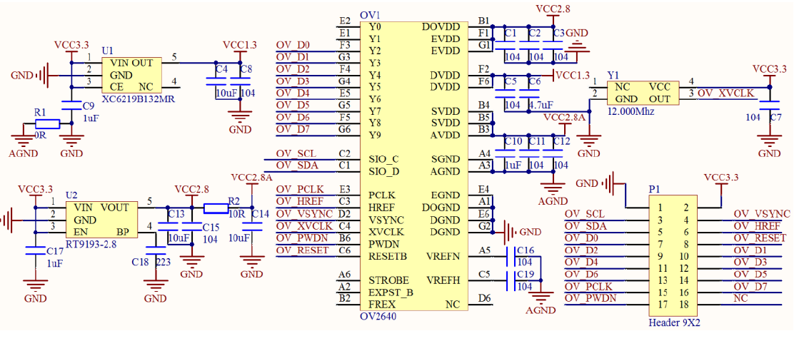
based on the schematics I get from seller, the internal schematics of the board is:

I assume there is no clock is required for this module and the clock of the module is provided by Y1 (I have opened the lens and check the Y1 output, it is 12MHz).
Is there anything I should do to read image from this module?
Any command I should send to the module?
and trying to make it work with my Zynq FPGA. I can read and write into it with SCCB protocol. When I read from address 0x15 (table 13) the COM10 register is 0x00, means PCLK is always output. However when I check the PCLK pin, there is no clock on it.
based on the schematics I get from seller, the internal schematics of the board is:
I assume there is no clock is required for this module and the clock of the module is provided by Y1 (I have opened the lens and check the Y1 output, it is 12MHz).
Is there anything I should do to read image from this module?
Any command I should send to the module?
