Continue to Site

Welcome to EDAboard.com

Welcome to our site! EDAboard.com is an international Electronics Discussion Forum focused on EDA software, circuits, schematics, books, theory, papers, asic, pld, 8051, DSP, Network, RF, Analog Design, PCB, Service Manuals... and a whole lot more! To participate you need to register. Registration is free. Click here to register now.

[SOLVED] Nmos Drain Spice Simulation and Hand Calculations Comparision

Status
Not open for further replies.

shabazsyed

Junior Member level 3
Joined
Dec 28, 2011
Messages
25
Helped
1
Reputation
2
Reaction score
1
Trophy points
1,283
Activity points
1,466
Hello Guys ,
I am trying to verify my Hand Calculations and Spice Results. But the simulated results are less than Calculated. Its TSMC .35um Tech.
Spice Code.
***8
vdg vds 0 dc 5
vff vgs 0 dc 5
vdum vds b dc 0

mn1 b vgs 0 0 nmos w=1u l=.4u

.include moslh.md
.dc vdg 0 5 .00005 vff 1 5 1
.control

reset

run

plot i(vdum)
.endc

.end


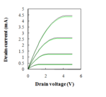
Capture.PNG
My Calculated Results
Capture.PNG
Simulated Results.
Y is Calculated Result differing From Spice Results?
Any Suggestions.
Eagerly Waiting For Some replies.
Thanx
 

Do you imagine that your hand calculations (and importantly
the underlying model) include all of the nonidealities of real
short-channel devices?

In my courses, back in the day, the first thing mentioned
was all of the assumptions made to render hand analysis
tractable.

If the SPICE model is matched to data then these aspects
are embedded, not neglected. Of course that requires
some trust in the foundry model.
 
Thanx for Reply. Ok i Guess u r saying that i am not considering various other Parameters for calculations, But i read on internet and from the various books that + or - 5% variations only happen between Spice and Hand Calculations even if i ignore those parameters. Is it because the technology is .35um and that square law formula holds only for Large devices. If it is, then how to go on designing Circuits @ this level because we need W/L for Particular current in circuit or Current Mirroring or so.. So how do i Decide it
 
  • Like
Reactions: junky1

    junky1

    Points: 2
    Helpful Answer Positive Rating
Capture.PNGCapture1.PNG
I made Some new improvements today , Now my calculated result is exactly Twice than what i simulated..... I suspect there is something wrong with my Model File.
 

I guess i am not considering velocity saturation effect and effective mobility right?
 

I guess i am not considering velocity saturation effect and effective mobility right?

Already apart from these (and other) effects, you can see deviations from your hand calculations which are by far larger than those you found: just by changing the gate length (keeping the same W/L ratio) -- at least in strong inversion operation, s. the foll. figure from David M. Binkley "Tradeoffs and Optimization in Analog CMOS Design" :


The a.m. book also trades extensively velocity saturation and VFMR (vertical field mobility reduction) effects, as well as CLM (channel length modulation) effect.
 

this is Y i had that NMOS model question. Coz i calculated drain current using level 1 eqn but simulations are done using level 49.... So i guess u r trying to tel me @ sub micron i cant calculate current and have to depend on simulators and my model? So how do designers calculate or find W/L ratio for a particular current in circuit? Thanks
 

... how do designers calculate or find W/L ratio for a particular current in circuit?

E.g. with extended "hand calculations" using Excel tables, s. the a.m. book!
 

Status
Not open for further replies.

Part and Inventory Search

Welcome to EDABoard.com

Sponsor

Back
Top