Continue to Site

Welcome to EDAboard.com

Welcome to our site! EDAboard.com is an international Electronics Discussion Forum focused on EDA software, circuits, schematics, books, theory, papers, asic, pld, 8051, DSP, Network, RF, Analog Design, PCB, Service Manuals... and a whole lot more! To participate you need to register. Registration is free. Click here to register now.

Negative resistance oscillator, how to get rid of wrong high frequency of oscillation?

Status
Not open for further replies.

Terminator3

Advanced Member level 3
Joined
Feb 25, 2012
Messages
802
Helped
71
Reputation
142
Reaction score
63
Trophy points
1,308
Activity points
9,027
Negative resistance oscillator, how to get rid of wrong highfrequency of oscillation?

I am following RF design book and tutorials on negative resistance oscillator, but encounter some problems.

My design is 5GHz oscillator. I want to use single device, so i decided to use NE3210S01, it has very high gain, there are many papers with push-push, etc. oscillators, where NE3210S01 fundamental oscillation is at 3...9 GHz. My idea is that this device can give good harmonic level at 10GHz.

So i use this approach: take s-parameters at 5GHz, check for stability factors, add inductance if needed, update S-parameters in new configuration. Then choose Gsource near to inverse of S11, calculate Gout and decide Gload, correct Gload. Check that Gsource and Gload are in unstable regions. Problem is that in transient simulations i currently obtain some unwanted result like 11 to 15 GHz.
So it looks like Gin*Gs=1, Gout*Gload=1, k<1 conditions are matched at those higher frequencies.

I came to a conclusion, that i must draw all stability circles from 1 to 20 GHz, and draw Gload-Gsource impedance points too, and check all frequencies for instability. Actually there must be some wide band analysis, like building stable LNA. But it is pretty odd, because i come to conclusion that series and shunt resistances must be added to make transistor stable at 9..15GHz. Why i think it is strange, because authors who used NE3210S01 in oscillators (push-push, etc.) did not use any series resistances. I am pretty sure that transient simulation is correct, because it gives good results for book examples. Also gain and unstability factor at frequencies above 10GHz is too high.

What tools would you use to analyze such oscillator problems?
 

Re: Negative resistance oscillator, how to get rid of wrong highfrequency of oscillat

you can chose a transistor with a little less high frequency gain. Or you can do something to resistively shunt energy to a load at high frequency. The problem is you get small microresonances in things like bias lines, etc, and they can make the device latch on and oscillate at those high frequencies. You need to kill the system gain at the high frequency somehow
 
Re: Negative resistance oscillator, how to get rid of wrong highfrequency of oscillat

I tried configuration without inductive stub (common source), and high frequency oscillation disappeared.
What analysis i can do to ensure that wrong frequency does not occur?
Should i check all Gs, Gl, stability circles, stability factor for all frequencies up to Ft (Ft/2?).
Or maybe check negative resistance value for all frequencies?
 

Re: Negative resistance oscillator, how to get rid of wrong highfrequency of oscillat

I ensured that oscillator is at least conditionnaly stable at all unwanted frequencies. I did it by choosing source and load imedances in a such way, that they are pretty far away from unstable borders over frequency range 1-20GHz. I found out very interesting thing, that by calculating all distances on a smith chart it is possible to analyze manufacturing tolerances influence on stability (by building plots of those distances). For example, if some resistor or inductance value varies, circuit can become unstable. Plotting such distances gives frequency "peaks" where attention must be paid. So i optimized it till point, that there is very good negative resistance at 5GHz, reflection coefficient meeting oscillation condition, but oscillator does not work. Then i learned about nyquist plots, and that mine goes in counter clockwise direction or does not include 1+j*0 point, which does not satisfy oscillation criteria.
 
Last edited:

Re: Negative resistance oscillator, how to get rid of wrong highfrequency of oscillat

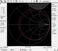
Plotting the stability circles for the provided S-parameters of NE3210S01 can be seen that the transistor is potential unstable in 1GHz-7GHz frequency range.
Making stable to use as an LNA perhaps is not a problem, but to make it stable and then to make it oscillating could be a challenge.

 
Re: Negative resistance oscillator, how to get rid of wrong highfrequency of oscillat

Maybe i am overthinking it:
I want to eliminate common source vias (problems with PCB thikness fr4 tolerances, via size/conductance tolerances). I feel vias will give problem, because small variation of source to ground path length leads to rapid movement of stability circles to the point where ~10..14GHz oscillations occur. So all negative resistance design fails when i make small variations of source-to gnd path. Although it seems that very good 10GHz negative resistance oscillator is possible that way.
To eliminate vias, i want to use open source stub with thin biasing line with quarterwave stub to ground.
I like ne3210s01's high gain, so going to try a little more.
here is my old 2015's experiment on S-parameters:

https://www.edaboard.com/threads/339788/
there was an annoying problem: small rounding errors can lead to huge stability circle movement.
Now i ever thinking about putting varactor not only in gate network, but also on source pin to make design more flexible.
 

Re: Negative resistance oscillator, how to get rid of wrong highfrequency of oscillat

Very interesting:
Therefore, the general Nyquist stability criterion (whichfor stable systems with no open-loop poles in the RHP doesnot allow such an encirclement) indicates instability of thecircuit in Fig. 2. However, as explained before, the circuitwill not produce self-sustained oscillations.Thus, it can be concluded that a Nyquist plot for the loopgain can be used only as an indication if the closed-loopsystem will be stable or unstable in a general sense—thatmeans, if the system will be asymptotically globally stable(bounded output for bounded input). However, in contrastto the conclusions as formulated in [1], this stability cri-terion cannot provide any reliable information about theability of a circuit to oscillate.

On the Barkhausen and Nyquist stability criteria (PDF Download Available). Available from: [accessed May 11, 2016].
also i readed http://www.highbeam.com/doc/1G1-56015068.html

And:
This example, therefore, reconfirms that the Barkhausencriterion is only a necessary but not a sufficient oscillationcondition. In addition, the Nyquist stability criterion in itsgeneral form only indicates instability but cannot provideany information if this instability will cause oscillations ornot. Thus, there seems to be still no compact formulation ofan oscillation criterion that is both necessary as well assufficient.In this context, some further analyses are in progress;results will be communicated later.

On the Barkhausen and Nyquist stability criteria (PDF Download Available). Available from: [accessed May 11, 2016].
Pretty interesting reading. Many RF books do not mention Nyquist stability criteria.
 

Re: Negative resistance oscillator, how to get rid of wrong highfrequency of oscillat

Almost the entire book "Discrete Oscillator Design" written by Randal Rhea is based on this concept:

https://www.amazon.com/Discrete-Oscillator-Design-Nonlinear-Transient/dp/1608070476

There you can find the most comprehensive explanation for negative resistance oscillators.

Unfortunately this concept doesn't make always a circuit to oscillate, which basically is the most important (and first thing that have to get) in oscillator design.

In my opinion is important in oscillator design to go deep in theory for: low phase noise, high frequency stability, low spurious emissions, but NOT for starting the oscillation.
 
Re: Negative resistance oscillator, how to get rid of wrong highfrequency of oscillat

I will post if get some results. Want to share something: I found few references to Alechno’s virtual ground circuit transformation technique, here is some link to mwrf.com in this topic: https://www.edaboard.com/threads/10100/ but it seems that article does not exists online anymore. But i found some interesting article by Alechno: **broken link removed**
The judgement depends on criterion accepted, and
this is bound with question: what is the subject here? The answer must be: it is the noise. As this is really
an agent which works in an oscillating circuit. And there is always the particular point in the circuitry,
which chosen as a reference shows where and how this factor acts. That is indicating how the noise is
magnifying and circulating in the loop. Such a reference point truly deserves to be called as virtual or
essentially true one. The actual PCB arrangement states completely different matter, tending rather to fade
away the loop like in Fig.2a. The practical advantages of such implemented „artificial” ground are obvious:
microstrip resonator is plainly arranged, low-inductance emitter grounding is not required, load connection
is simple.
 
Last edited by a moderator:

Re: Negative resistance oscillator, how to get rid of wrong highfrequency of oscillat

I have a question regarding Rload=-Rout/3 rule of thumb. For example "RF Circuit Design Theory and Applications" (Reinhold Ludwig, Gene Bogdanow): it is said than Rin becomes less negative with increasing output power, when oscillator start ups.
I am uncertain about some details.
For example, with 1-port negative resistance device such as gunn diode, it is pretty obvious:
we calculate Zload as Zload=-Zoutput. Then make newRload=Rload/3.

But for two-port device (BJT, FET) i am not so sure.
As we choose Rload=-Rout/3, should not we recalculate Ginput based on that new Gload?
I read many papers on negative resistance oscillators, and there always some uncertainity about what is called LOAD, what is SOURCE, what is Termination. Sometimes Gload is resonator, and oscillator is "loaded" with resonator. Sometimes resonator is termination, so it is "terminated" with resonator.

For example:

**broken link removed**
Example 11-9
They choose real part of Zload=-Rin/3
Zload is at source pin of FET (common gate configuration)

and example in the boog "RF Circuit Design..." i mentioned before:
Example 10-5
They choose real part of Zload=-Rout/3 (actually a little smaller)
Zload is at drain pin of FET!

Both configurations are the same - commong gate FET oscillator. But in first case (variable names as in second book) Zinput is corrected. Is it arbitrary choosen which of termination corrected with this rule of thumb?

Which one to use, Rload=-Rout/3 or Rsource=-Rin/3?
 

Status
Not open for further replies.

Part and Inventory Search

Welcome to EDABoard.com

Sponsor

Back
Top