Continue to Site

Welcome to EDAboard.com

Welcome to our site! EDAboard.com is an international Electronics Discussion Forum focused on EDA software, circuits, schematics, books, theory, papers, asic, pld, 8051, DSP, Network, RF, Analog Design, PCB, Service Manuals... and a whole lot more! To participate you need to register. Registration is free. Click here to register now.

need help with basic OTA calculations

Status
Not open for further replies.

kalinowskikswonilak

Newbie level 2
Newbie level 2
Joined
Sep 16, 2010
Messages
2
Helped
0
Reputation
0
Reaction score
0
Trophy points
1,281
Activity points
1,299
It's my first post so hello everybody.

Firstly, I'd like to say that I'm real nwb as far as analog IC design is concerned and I have some really basic questions:

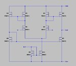
I'd like to calculate parameters(W/L) of transistors to achieve transconductance of the simpliest ota(schematic attached) around 100mS. No other requirements, technology 0.35um.

I've already briefly read Analog design essentials and Allen Holberg book but honestly I have no idea where to start to calculate dimmensions of transistors.

Any help and sample calculations would be greatly appreciated.

ps. I've read several ee240 reports but they're way too complicated for such a simple project as mine.

cheers,
michal
 

Attachments

  • simple_ota.jpg
    simple_ota.jpg
    43 KB · Views: 168

The link posted by erikl works great, but I never liked that artical for some reason...
I like the approach of Paul r. Gray (Similar, but not exactly the same).
You can check out an over view of the artical **broken link removed**
Hope this helps.

Edit: And also, if memory serves me right, the gm/Id artical does not deal with compensation capacitor and resistor, which are usualy kind of a big deal for two stage Op Amps.
 
Your amplifier is not a 2 stage one strictly speaking. It has only one high-impedance node (the output) and the diff-pair itself does not provide a lot of gain since it is loaded by diode connected transistors. Compensation is also done differently compared to the two-stage Miller compensated OTAs. Here you compensate with the load capacitor. This being said, 100mS of transconductance seems quite a lot for 0.35u CMOS. But, here's how I would think about it. I also assume that by transconductance you mean the output current of the OTA vs the input diff voltage. Whatever current you get from the output splits in 2 and gets divided by the ratio of M2-M3 (M4-M5). So, the current the diff pair has to produce is smaller by that ratio - say 10 times. The transonductance of the input transistor is then 10mS. Since you don't say anything about BW requirements, I assume it is not important. Then, you can fix the Vov of the input devices which is something like 2/gm/Id and since you know how much gm you want, you find Id. Choose L and find W. Or you can fix the current you want to consume, then find gm/Id and for a given L you can get Id/W and from here W. In all this I assume you are familiar with the gm/Id design methodology. If not then for the above two approaches you use the square low transistor formulas. I also want to mention that many times for this topology a mirror ratio of 10 (M2-M3; M4-M5) is a lot for many reasons. 2-5 is more likely. Then you diff pair transistors have to provide bigger transconductance.
 
Last edited:
thank you all for your posts. I was familiar with the two papers that were posted, but I'm gonna have to read few more times what sutapanaki has written. I'll get back to you guys with some more questions and sample calculations.

thanks a lot again
michal
 

Since it's an one-stage op-amp effectively, the transconductance is simply the one of the input transistors.
If you go for weak inversion gm=Id/(n*Vt), independent of W,L. You get the maximum gm/Id ratio here.
If you go for strong inversion gm=sqrt(2*beta*Id), where beta=μ*Cox*Kn.
 

Status
Not open for further replies.

Part and Inventory Search

Welcome to EDABoard.com

Sponsor

Back
Top