Continue to Site

Welcome to EDAboard.com

Welcome to our site! EDAboard.com is an international Electronics Discussion Forum focused on EDA software, circuits, schematics, books, theory, papers, asic, pld, 8051, DSP, Network, RF, Analog Design, PCB, Service Manuals... and a whole lot more! To participate you need to register. Registration is free. Click here to register now.

Need help for an inverter layout

Status
Not open for further replies.

ardique

Junior Member level 2
Joined
Aug 29, 2007
Messages
23
Helped
1
Reputation
2
Reaction score
1
Trophy points
1,283
Location
Taipei
Activity points
1,484
Hi all,

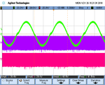
I'm currently work on a 1kVA full-bridge single phase inverter with SPWM current control. However, during my testing on open loop with lower rating test (60Vdc, Rload = 11.6ohm, Irated = 3A), I have problem at my high side switching pair (Q3). Attached are the schematic, pcb layout design and the waveform that I measure on Vgs on Q2(pink color) and Q3(purple color). Since the problem is occurred at pair of Q2&Q3 that I'm working with. Please let me know what did I missed or wrongly do the connection.

I'm using CoolMOS power transistor (SPW35N60C3), MINMAX(MCW03-24D15), gate driver (TLP350).

Moreover, the spwm signal generated from DSP also affected by the distortion as shown in waveform.

Your cooperation is very much appreciated.

Thank you.
 

Attachments

  • power stage schematic.pdf
    255.5 KB · Views: 213
  • power stage layout.pdf
    124.9 KB · Views: 211
  • vgs3vgs2.png
    vgs3vgs2.png
    34.2 KB · Views: 205

Hi,

Usually every Mosfet manufacturer, IGBT manufacturer, driver IC manufacturer has design notes about PCB layout.
Basics can even be found in every of these devices' datasheets.
There are many other threads where the PCB layout problems are discussed in detail.

In short:
* Use a solid GND plane, no copper pour.
* think that every signal is a (HF) loop. E.g.: It's not only the signal from driver to Mosfet, there has to be a return path for the current. You always have to route the return path with the same care as the initial signal. Here a solid GND plane makes life easier.
There are threads with detailed descriptions and pictures.

Klaus
 
Last edited:
The waveforms are far from being self-explanatory. What is intentionally driven by the controller, what is unwanted noise or crosstalk?

- - - Updated - - -

Q2 and Q3 don't form a pair, according to the schematic they are LS1 and HS2 gate signals. What's driven to HS1 and LS2 during the same time?

How do you probe floating HS gate signals?

- - - Updated - - -

Moreover, the spwm signal generated from DSP also affected by the distortion as shown in waveform.

How do you conclude this? It's quite difficult to acquire an "unaffected" waveform in a power electronics system. Seeing spikes in a particular waveform doesn't mean that they are actually there.
 
I see Q2/Q3 as a pair in a basic classD scheme providing positive voltage and Q1/Q4 providing negative voltage.

Ok after staring for a few minutes I see
-Isolated gate drivers for every fet
-One isolated supply shared for gate drive 2 and 4 (ok)
-With individual isolated supplies for 1 and 3 (good)

That all checks out for me. Questions:
-Why are you using +15/-15
-What's the DC bus voltage
-How are you measuring the high side gate drive with the scope
 
Hi Klaus,

Thanks for your reply. Ok noted about the solid GND plane and will make an improvement on that.

Thank you.

- - - Updated - - -

Hi,

Thanks fo your reply. The controller is used to control the current of the inverter. However, as for the preliminary test, I'm using an open-loop where the controller will generate a constant spwm signal to turn on and off the switchs.

Sorry for my bad explaination. For this inverter, the controller will generated a pwm signal (epwm1A- for Q1&4, and epwm1B- for Q2&3) which the signals are active high complimentary signal. So the pair that I mention is for Q2&Q3 which have received the same signal to turn on/off.

For the HS gate signal, I'm using differential probe to measure it.

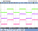
This is the condition when the DC supply (60Vdc) is not turn on. [yellow&green are for epwm1B (Q2&3) at the control board, purple Vgs2, and pink Vgs3]
scope_4.png

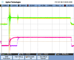
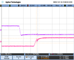
This is the condition when the DC suplly (60Vdc) is turn on.
scope_8.png

This is what I try said how the DSP signal also affected after the Dc supply is turned on, where suppose the DSP signal should be maintain, am I right?

Thank you.

- - - Updated - - -

Hi,

Thanks for your reply.
For your question:
-Why are you using +15/-15
> I'm using the +15/-15V because of the gate driver is required supply voltage 15 to 30V.

-What's the DC bus voltage
> For preliminary test, I'm using 60Vdc. In actual design is using 200Vdc.

-How are you measuring the high side gate drive with the scope
> I'm using the differential probe to measure the Vgs.

Did I answer your question correctly? Please let me know if anything is not correct.

Thank you.
 

Attachments

  • scope_6.png
    scope_6.png
    33.8 KB · Views: 192

Hi,

This is what I try said how the DSP signal also affected after the Dc supply is turned on, where suppose the DSP signal should be maintain, am I right?

FvM wrote:
Seeing spikes in a particular waveform doesn't mean that they are actually there.

To verify wheter the noisy signal is true or not, try this:
* setup is equal to the one before where you see the "noise" (60V applied)
* The only difference is: one probe tip of the DSP PWM signal should be connected to the connected to it's probe_GND. (Don't move the GND connection of the probe, leave it connected to the PCB_GND)

I expect you will still see noise at this channel. Although the input is short circuited and thus should be zero.

The noise is cause by
* probe GND currents (GND loop)
* induced noise

Klaus
 
The post#5 waveforms shine some light on the issue. It looks like the DSP control signals are maintaining the intended pattern. The superimposed high frequent spikes are probably measurement artefacts that are not actually send by the controller.

The TLP350 output shows however 2 - 3 µs dropouts. The most likely explanation is that the UVLO circuit is triggered by VCC spikes, which means that the capacitive bypassing is apparently insufficient. The waveform resolution is not suitable to see high MHz signals, but it might be that edges are oscillating.

Transmitting gate driver signals through cables often turns out problematic due to common mode crosstalk. We often ended up with differential signaling and massive common mode filters.

- - - Updated - - -

The TLP350 input RC filter might be contra productive by slowing down the edges. Also the asymmetrical wiring is probably not optimal. I would try with a twisted pair driving each TLP350 LED, supplemented by a common mode choke.
 
Crosstalk between PWM signal traces is negligible (post #5, DC supply unconnected).

Measure DC supply (60 V supply) noise (unconnected to the present system).
 
Measure DC supply (60 V supply) noise (unconnected to the present system).
Won't expect much noise here. The waveforms show crystal clear that the switching power stage itself generates the noise.
 
Can you ramp up the 60V or is it on/off? Ramping helps gather more information.

Scope noise would increase mostly proportionately.

A functional problem I'd expect to see it transition from none->intermittent->consistent as input voltage ramps up.


Still question the +15/-15V as that's an unnecessarily large gate drive in most applications, though probably unrelated to this particular problem.
 

I noticed a possible design problem. Is the PWM control voltage really only about 2V as indicated in post #5? If so, the required TLP350 input current won't be achieved. Could be a reason for drop out effects.
 

Hi all,

Thank you for all of your advice. I really appreciate it. I will look into them and will update you later.
 

Hi all,

After taking all of the advice, I have able to solve lots of the problems in my circuit even not fully solved but still have lots of improvement than before. Thank you so much.
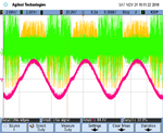
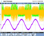
Below are the waveform that I measured before and after the troubleshoot.

Before the troubleshoot:
vload1.png

After the troubleshoot:
scope_13.png

Note: for both measurements, the channel 1&2 (yellow and green signal) are clipped at the DSP output pin using osc probe, while the sinusoidal waveform is measured at the output (Rload) using diff. probe.

As FvM and Klaus mentioned that those spikes might not actually there and might caused by the GND loop from the power stage and I have figured out some improper GND loop on the power stage. I will do the modification on the layout according to this problem.

Below shows the waveform that measured the Vgs1, Vgs3 and output voltage (VRload) using diff. probe. The spikes are not really bad, but it still exists in the signal, which it might caused by the improper GND loop on the power stage layout.
scope_4.png

scope_1.png
From this figure, the spike about 16.5V is occurring during the mosfit turned on. I hope this spike will be eliminated after the modification on the layout.

If there's some comment or suggestion please let me know.

Thank you.

- - - Updated - - -

Hi,

Can you ramp up the 60V or is it on/off? Ramping helps gather more information.

Scope noise would increase mostly proportionately.

A functional problem I'd expect to see it transition from none->intermittent->consistent as input voltage ramps up.


Still question the +15/-15V as that's an unnecessarily large gate drive in most applications, though probably unrelated to this particular problem.

I have try to ramp up the 60V, the noise is increasing as the DC voltage is ramp up simultaneously. Regarding the +15/-15V, I have take noted about it and also consider it in my modification. Thanks to you for that question.

- - - Updated - - -

Hi,

I noticed a possible design problem. Is the PWM control voltage really only about 2V as indicated in post #5? If so, the required TLP350 input current won't be achieved. Could be a reason for drop out effects.

Yes, thanks to you. I just noticed that in my design, the PWM signal is directly sent from DSP into the gate driver. That's why it will have a sudden drop which will cause the TLP350 input current is not sufficient for its input on-state current.

The DSP (TMS320F28335) only can produce 2.4V, whilst the measured at the output pin of PWM is 2.34V. After doing a simple calculation, there's only 5.67mA while the min input on-state current for TLP350 is 7.5mA.

Therefore, I will consider adding HEX inverter buffer before the TLP350 in the circuit.
Thanks.
 
Last edited:

Hi,

Schmitt-trigger buffer:
HC types (for 3.3V supply) have poor output drive capabilities.
HCT types (for 5V supply) ... the same.

Consider to use
* LCX14 or AC14 for 3.3V supply
* Or ACT14 for 5V supply.

Klaus
 
Hi,
Hi,

Schmitt-trigger buffer:
HC types (for 3.3V supply) have poor output drive capabilities.
HCT types (for 5V supply) ... the same.

Consider to use
* LCX14 or AC14 for 3.3V supply
* Or ACT14 for 5V supply.

Klaus

Okay noted. Thanks for the advice.
 

From this figure, the spike about 16.5V is occurring during the mosfit turned on. I hope this spike will be eliminated after the modification on the layout.
I presume, you are not able to probe Vgs exactly at the MOSFET pins. Thus it's still unclear, if the oscillating waveform exists at gate or it's mainly a common mode measurement artefact. If present, it would cause multiple MOSFET edges, high switching losses and EMI.

I suggest to increase the TLP350 LED current first and reevaluate the behavior.
 
I suggest to increase the TLP350 LED current first and reevaluate the behavior.

Okay, noted. Will make the adjustment on the TLP350 first and reevaluate the behavior. Thanks for the advice.
 

Status
Not open for further replies.

Part and Inventory Search

Welcome to EDABoard.com

Sponsor

Back
Top