Continue to Site

Welcome to EDAboard.com

Welcome to our site! EDAboard.com is an international Electronics Discussion Forum focused on EDA software, circuits, schematics, books, theory, papers, asic, pld, 8051, DSP, Network, RF, Analog Design, PCB, Service Manuals... and a whole lot more! To participate you need to register. Registration is free. Click here to register now.

Need advice on SMD connector adaptation to 2.54mm pitch connector

Status
Not open for further replies.

michcfr

Advanced Member level 4
Full Member level 1
Joined
Mar 7, 2012
Messages
106
Helped
0
Reputation
0
Reaction score
0
Trophy points
1,296
Activity points
2,011
Hello,

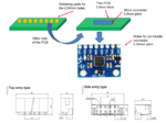
I want to connect an existing PCB (the blue PCB on the picture) made for 2.54mm pitch header connector to a micro SMD connector of 0.8mm pitch. See the dimensions of this connector at the bottom of the figure. B is 10.2mm.
My first idea is to design a tiny PCB on which one side is soldered with the SMD microconector and the other side with pads that can be soldered to the 2.54mm holes of the blue PCB.

Do you think that this solution would work? I don't know how to solder the pads to the 2.54mm holes? Any suggestion?

Any optimization or alternatives are welcomed :)


in advance, thank you

Michel
connector adapter.png
 

Soldering pads are not necessary.Instead, use a 2.54 pitch simple header ( board-to-board) then solder tiny SMD connector to this additional PCB.
Simpler..
 

Soldering pads are not necessary.Instead, use a 2.54 pitch simple header ( board-to-board) then solder tiny SMD connector to this additional PCB.
Simpler..

Thank you BissBoss for the suggestion.

I need the height of the assembly to be as thin as possible: around 5mm. Sorry to forget this detail.
Standard 2.54mm pin headers are of 7mm height that is too much thick. Unless you know special flat models?

thx
 

You didn't tell how much lateral (horizontal) room is available. Also, is it assembly of a few prototypes or larger quantities? With sufficient room, I would use edge metallized pads. Reflow soldering of bottom pads could work, too.
 

You didn't tell how much lateral (horizontal) room is available. Also, is it assembly of a few prototypes or larger quantities? With sufficient room, I would use edge metallized pads. Reflow soldering of bottom pads could work, too.

Thank you FvM for your help.
I don't have lateral space.
For the moment it is for prototypes purpose but I would like to use the same technics for large quantities.

The existing (blue) PCB do not have edge metallized pads/castellated PCB, so I don't see how to it to the other PCB
If I make the green PCB with edge metallized pads, how can I solder edges with the 2.54mm holes of the blue PCB?


If I make the green PCB with edge metallized pads, how can I solder edges with the 2.54mm holes of the blue PCB?
On top of the pin header pads.

- - - Updated - - -

but I would like to use the same technics for large quantities.
Isn't it cheaper to redesign the blue PCB?
 

On top of the pin header pads.
- - - Updated - - -


ok, I see. Thank you.

- - - Updated - - -
Isn't it cheaper to redesign the blue PCB?

I don't know yet, but the blue PCB is something widely spread in the Chinese market (Alibaba) for few $ and there are many other type of blue PCB I have to adapt in the same way.
I think that the total cost is higher because of the "wasted" time for the blue PCB part realisation: sourcing components, design the PCB, assembling, testing.... in addition there are: stock mgt, leading time issues....

"Patching" the blue PCB seems to be the best strategy. Does it makes sense?

- - - Updated - - -


Thank you BigBoss
This connector is 8.3mm height. Nothing more flat? 4mm or less?
 

Status
Not open for further replies.

Part and Inventory Search

Welcome to EDABoard.com

Sponsor

Back
Top