Continue to Site

Welcome to EDAboard.com

Welcome to our site! EDAboard.com is an international Electronics Discussion Forum focused on EDA software, circuits, schematics, books, theory, papers, asic, pld, 8051, DSP, Network, RF, Analog Design, PCB, Service Manuals... and a whole lot more! To participate you need to register. Registration is free. Click here to register now.

[SOLVED] Need a suggestion on this PCB design

Status
Not open for further replies.

tajiknomi

Member level 4
Member level 4
Joined
Nov 2, 2015
Messages
79
Helped
0
Reputation
0
Reaction score
0
Trophy points
6
Activity points
754
I am a noob in PCB design and would like to know about the common mistakes beginners do while designing PCB. Here is a simple PCB which i had made.

1.JPG

The problem I am facing is that the connector on the bottom is NOT ON THE EDGE as shown here

2.png

If I drag these connectors down, the only problem which I am a concern of is that PCB will not look good because i have to remove the trace-pattern and I don't want to do that :smile:
 

The loops from your resistors to your connectors are largely unnecessary, as a straight down rout would work better. It is usually a good idea to keep traces as short as possible.

You say that "the connector on the bottom is NOT ON THE EDGE", but we don't have any context as to what you mean.

There are no mounting holes. How did you plan on mounting the board?

I'm thinking that there should be a capacitor somewhere on the board, but without a schematic, that is just a guess.

Try not to use right angles in any of your routs. Try to keep your angles in mutiples of 45°. Most packages give an option to "set miters".

Make your traces as large as you can, but no larger! This keeps the inductance of long traces lower.

Your right outline is not orthogonal. Usually, this is what the PCB house uses to generate a cutout rout.
 
The board can be condensed; you should try to reduce to total conductor length and leave all the margins on the side.
 
The loops from your resistors to your connectors are largely unnecessary, as a straight down rout would work better.

You are right but my obsession was that the PCB trace pattern should look good :)

"the connector on the bottom is NOT ON THE EDGE", but we don't have any context as to what you mean

What i mean by this is that the connectors are not close to the edge of the board.

Try not to use right angles in any of your routs. Try to keep your angles in mutiples of 45°

That's what I thought about first but by surfing different threads about 90/45-degree dilema i realized that it really doesn't matter in low-freq signals.

Make your traces as large as you can, but no larger! This keeps the inductance of long traces lower
+1

There are no mounting holes

There are mounting holes but I have disabled it layer.

I have customized my design a little and it comes out to be like this

Capture.JPG

you should try to reduce to total conductor length and leave all the margins on the side
+1
 

As you probably found out, it makes sense to place components first and then route the connections.

You are right but my obsession was that the PCB trace pattern should look good :)
I won't associate the useless trace detours in the original layout with "looking good". Similarly, the second attempt would look better if you route the traces as direct as possible, mitering traces as usual. I don't see the purpose of the large unconnected copper pours.

I presume the board should have mounting holes.
 

Your second board is better. I always use copper ground pour, because it will keep the noise down. You might consider using a double sided board, with the back side just one big copper ground plane, then use vias to connect the top and bottom pours. Also, this will allow you to move your connectors closer to the edge.

Your obsession with "making the board look good" may be at the expense of extra noise. If you provide separatation for your traces at the bottom, you will be able to pour ground copper between them.

You should get into the habit of using mitered corners all the time. One, it makes the board look professional (you'll be hard pressed to find a professionally routed board with unnecessary 90° corners). And two, a mitered corner is easier for the PCB vendor to produce (there is sometimes over-etching at a 90° corner).

One more thing - the trace widths for the bottom parts should be increased in width. I'm assuming that this is some kind of LED display board and that these traces are to the LEDs. If so, then remember that LEDs will draw enough current to create a voltage drop along your traces. Increasing the width will greatly reduce this drop.
 
Last edited:

There are no mounting holes. How did you plan on mounting the board?
I presume the board should have mounting holes

Oops, I forgot that; I will add them now.

I don't see the purpose of the large unconnected copper pours
Pour is used as a ground in the above case.

If you provide separation for your traces at the bottom, you will be able to pour ground copper between them
One more thing - the trace widths for the bottom parts should be increased in width.Increasing the width will greatly reduce this drop
+1

On your helpful suggestions, I have modified the design as follows.
Capture.JPG

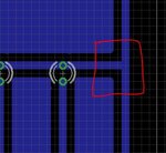
How can i solve this Right angle ?
Capture.JPG
 

How can i solve this Right angle ?

That's a "T" and it is acceptable.

- - - Updated - - -

The middle connector at the bottom has an overlap issue. And I still think that you should miter all your traces.
 
It is always a good practice do not route with any other angles than 0/45/90 degrees; it is not an issue for the thick traces above.
 

The rightmost components needs some cleanup- the pads are touching OR move the traces.

The traces to the switches (??) can be fatter- why so thin?

You need to put a text stating some ID/LABEL/MODEL/VERSION/DATE etc etc.

The lines connecting to the connector (traces connecting to the resistors) may be converted into vertical +45 deg lines.

Rest are ok in my opinion.
 

Someone suggested to bevel the "T"

Not necessary to bevel the "T".

I think all the traces are mitered now

"Miter" means that all traces are routed in multiples of 45°. Routing as your latest image shows is giving you clearance issues (some traces are too close to vias, or other traces).
 

"Miter" means that all traces are routed in multiples of 45°....

And, to be technically perfect, only multiples of 0, 1 and 2 are permitted in a PCB track... For RF work, use rounded or circular bends if you want to take a turn...
 

Status
Not open for further replies.

Part and Inventory Search

Welcome to EDABoard.com

Sponsor

Back
Top