Continue to Site

Welcome to EDAboard.com

Welcome to our site! EDAboard.com is an international Electronics Discussion Forum focused on EDA software, circuits, schematics, books, theory, papers, asic, pld, 8051, DSP, Network, RF, Analog Design, PCB, Service Manuals... and a whole lot more! To participate you need to register. Registration is free. Click here to register now.

N Channel and P Channel MOSFET symbols

engr_joni_ee

Advanced Member level 3
Joined
Nov 3, 2018
Messages
822
Helped
2
Reputation
4
Reaction score
7
Trophy points
18
Activity points
6,875
Hello,

In MOFET devices, the channel is established between Drain and Source when a certain voltage is applied at the Gate, is that true ?

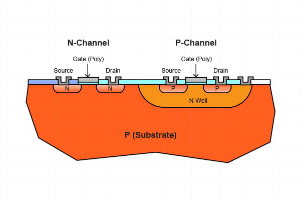
The channel is made of P-Type material in PMOS and the channel is made of N-Type material in NMOS, right ?
--- Updated ---

In the following link, the symbols in Figure 1 are wrong ?

The symbols in Figure 4 and Figure 6 are ok. Please confirm. Thanks in advance.
 
1) canonically true, but the value and slope vary

2) Backwards, PMOS body is N- (so as to diode-
block P+ drain from P+ source, until channel is
made); NMOS, flip it.

3) There are multiple "accepted" symbolizations of
the MOSFET. Digital and analog and power seem to
prefer differently. The ones you linked appeal to me
as "an old bipolar guy". Sometimes you will see the
arrow applied to the B terminal instead, and in either
case the arrow informs you of the diode polarity - if
you look at it right.

Plain digital, you might only see 3T symbols and a
bubble (invert) for polarity with the body being an
assumed or inherited connection.
 
The Fig. 1 symbols look inpropriate to me. Unlike bulk terminal, there's no junction involved with D and S terminals, they are ohmic contacts to the channel. I didn't notice yet this symbol type in literature.
 
Hi,
the channel is established between Drain and Source when a certain voltage is applied at the Gate, is that true ?
This technically is not correct. The voltage has to be applied between GATE and SOURCE. That´s why it is called V_GS (and not V_G)

Now you may call me picky. But indeed this is one of the most often made mistake.
See here (just a couple days ago): https://www.edaboard.com/threads/mosfet-load-switch-circuit-overheating.411156/post-1774470
We frequently can see this here in this forum.

Klaus
 
There is always several schools, because everything is a matter of convention.
I was learned to draw gate close to source (like in JFETs) and distinguish between enhanced mode (or induced channel) and depletion mode (or built-in channel) by drawing solid or dashed line at channel. Some others (I believe US West Coast) developed symbols with gate on the center of symbol to make an analogy to BJT. In addition, for IC design were number of choice is limited, symbols become simplified and line for gate was used to distinguish between core and I/O devices.

In general, one would say that symbol does not matter as long as everyone understand it. However, as everything has consequences, usage of simple "digital style" symbol might lead to misunderstanding of device asymmetry or something else.
 
I draw JFETs with a centered gate because in my IC technologies I have only seen symmetric device structures.

Some like GaN are engineered with more complex drain features and are not S/D swappable.
 

LaTeX Commands Quick-Menu:

Similar threads

Part and Inventory Search

Welcome to EDABoard.com

Sponsor

Back
Top