mssong
Junior Member level 2

My t flip flop is not working.
It could be a very simple problem.
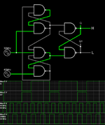
Below is the schematic of the t flip flop and on the right is the simulation result.
I have an input of 1, and I need to create a logic circuit that changes the signal level of the previous stage from 1 to 0 or 0 to 1 whenever CLK comes in, so I decided that a T FLIP FLOP would be a good choice, but it doesn't work.
What is the problem?


I solved it with the following structure
It could be a very simple problem.
Below is the schematic of the t flip flop and on the right is the simulation result.
I have an input of 1, and I need to create a logic circuit that changes the signal level of the previous stage from 1 to 0 or 0 to 1 whenever CLK comes in, so I decided that a T FLIP FLOP would be a good choice, but it doesn't work.
What is the problem?
--- Updated ---
My t flip flop is not working.
It could be a very simple problem.
Below is the schematic of the t flip flop and on the right is the simulation result.
I have an input of 1, and I need to create a logic circuit that changes the signal level of the previous stage from 1 to 0 or 0 to 1 whenever CLK comes in, so I decided that a T FLIP FLOP would be a good choice, but it doesn't work.
What is the problem?
I solved it with the following structure
Last edited: