Continue to Site

Welcome to EDAboard.com

Welcome to our site! EDAboard.com is an international Electronics Discussion Forum focused on EDA software, circuits, schematics, books, theory, papers, asic, pld, 8051, DSP, Network, RF, Analog Design, PCB, Service Manuals... and a whole lot more! To participate you need to register. Registration is free. Click here to register now.

My FPGA board layout, any comment?

Status
Not open for further replies.

zsuhh

Junior Member level 3
Joined
Jan 29, 2014
Messages
28
Helped
3
Reputation
6
Reaction score
3
Trophy points
3
Activity points
179
Placement layer:
Placement.jpg

Top layer:
Top.jpg

Gnd layer:
Gnd.jpg

Power layer:
Power.jpg

Bot layer:
Bot.jpg
 

Hi,

Please let me know, which FPGA you are using. what are the voltage levels?
 

Hi,

Are there diff pairs on the bottom?
If so they cross split planes on layer 3 that is not right.
They must see a constant gnd or power plane.
 

No any diff pairs on the bottom.
 

If the two connector pairs on above and bellow side are not being used for fastening purpose and it is expected connect for instance a flat cable, you could keep them apart due the edge of one may overlap the space needed to connect the other cable.
 

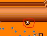
OK - whats this?
pic1.JPG

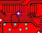
Move the tracks circled in black down so the via circled in blue can be moved so the loop in the track in the top pic can be removed.
pic2.JPG

I'm not so sure it's a good idea to have copper pour on BGA pads
pic3.JPG

It always take another pair of eyes to spot something small that could be better.
What software was this done in?
 
  • Like
Reactions: zsuhh

    zsuhh

    Points: 2
    Helpful Answer Positive Rating
Thank you very much. I am using allegro to layout.

- - - Updated - - -

spartan 6. voltage is : 3.3v, 1.2v, 1.8v
Hi,

Please let me know, which FPGA you are using. what are the voltage levels?

- - - Updated - - -

Thank you very much. I am using allegro to layout.

OK - whats this?
View attachment 119090

Move the tracks circled in black down so the via circled in blue can be moved so the loop in the track in the top pic can be removed.
View attachment 119089

I'm not so sure it's a good idea to have copper pour on BGA pads
View attachment 119088

It always take another pair of eyes to spot something small that could be better.
What software was this done in?
 

Status
Not open for further replies.

Part and Inventory Search

Welcome to EDABoard.com

Sponsor

Back
Top