Continue to Site

Welcome to EDAboard.com

Welcome to our site! EDAboard.com is an international Electronics Discussion Forum focused on EDA software, circuits, schematics, books, theory, papers, asic, pld, 8051, DSP, Network, RF, Analog Design, PCB, Service Manuals... and a whole lot more! To participate you need to register. Registration is free. Click here to register now.

Multiple external dataflash connected to MCU how to?

Status
Not open for further replies.

neazoi

Advanced Member level 6
Joined
Jan 5, 2008
Messages
4,148
Helped
13
Reputation
26
Reaction score
15
Trophy points
1,318
Location
Greece
Activity points
37,119
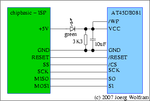
In the image attached the Green block is an ATMEGA644 and the blue is a AT45DB081 flash.
They are connected using the ISP of the MCU.

How can I connect a second identical flash to the ISP (and possibly other devices) and being able to select each of them with the use of a jumper switch?
 

Attachments

  • dflash_scheme.png
    dflash_scheme.png
    5 KB · Views: 125

Hi,

with SPI you should use inidvidual /CS signals to select different devices.


Klaus
 
  • Like
Reactions: neazoi

    neazoi

    Points: 2
    Helpful Answer Positive Rating
Hi,

with SPI you should use inidvidual /CS signals to select different devices.


Klaus

I was thinking of using the SS signal of the micro (in the green block) and connect it to the particular flash chip every time. Then leave the /CS pin of the rest of the flash chips unconnected.

Will that be enough or do I need to isolate the other signals of the SPI as well?
 

Hi,

Then leave the /CS pin of the rest of the flash chips unconnected.
General rule:
Never leave any (unused) input floating.

Now the question is: is the /CS pin pulled up? Or is it floating?

Klaus


nCS isn't pulled up internally, you need to provide external pull-up resistors for unconnected nCS pins.

The schematic in post #1 drives the SPI signals by 5V logic. I don't expect that AT45DB081 has 5V tolerant inputs.
 
  • Like
Reactions: neazoi

    neazoi

    Points: 2
    Helpful Answer Positive Rating
Hi,

You mean internally? I am not sure here is the datasheet
Either internally or externally. You just need to prevent it from floating.

If pullup is not mentioned in the datasheet...then most probably there is no internal pullup.

Klaus
 

Hi,


Either internally or externally. You just need to prevent it from floating.

If pullup is not mentioned in the datasheet...then most probably there is no internal pullup.

Klaus

Ok, but my point is, is the /CS alone enough to prevent simultaneous chips into the same ISP to interact with each other? There is a LED and a resistor that forms a potential divider to feed the chip with vcc, perhaps I should also cut off this?
 

Hi,

VCC and signal voltages need to be within their specified ranges.
(Did you mention voltages before?)

Did you read post#6?

The LED controlled power supply is a cheap and dirty solution.
This is not my style of designing circuits.

Try to solve it on your own:
Find the lowest power supply current from the flash datasheet.
Add the resistor current.
Find the voltage drop of the LED according it's datasheet.
Use the highest expectable 5V supply voltage
--> to find max flash supply voltage

Find the highest power supply current from the flash datasheet.
Add the resistor current.
Find the voltage drop of the LED according it's datasheet.
Use the lowest expectable 5V supply voltage
--> to find min flash supply voltage

Check if this meets the flash specification.

****
Also check V_OH range and and V_IH ranges of all communication partners if they meet specifications.

Klaus
 

nCS isn't pulled up internally, you need to provide external pull-up resistors for unconnected nCS pins.

The schematic in post #1 drives the SPI signals by 5V logic. I don't expect that AT45DB081 has 5V tolerant inputs.

It must have, because it works. This is not my schematic.
I could include jumpers for all signals and switch them off, then switch the other's chips jumpers on to select these other flash chips. But I thought that the /CS will be enough to swhitch it on/off to select the chip. I guess I will have to test it with multiple chips, I thought the answer would be straight forward, but I guess it isn't.
 

/CS = high effectively disables any input or output to the IC. It is active low, that's what the '/' tells you so to disable it the pin has to be pulled high to VDD. The remaining pins can stay connected as they are. Use a pull-up resistor on both /CS pins so no matter which is disconnected by the jumper is disabled. The resistance isn't critical, I would suggest 10K would be adequate as the /CS pin draws negligible current and the ATMEGA should be capable of sinking several mA.

I really wouldn't use that LED voltage dropper though, it is asking for problems, especially as the current drawn by the flash will vary quite a lot depending on whether it is reading, writing or idle. it isn't only the supply pin that should be 3.3V, the control signals should be 3.3V as well.

Brian.
 
  • Like
Reactions: neazoi

    neazoi

    Points: 2
    Helpful Answer Positive Rating
/CS = high effectively disables any input or output to the IC. It is active low, that's what the '/' tells you so to disable it the pin has to be pulled high to VDD. The remaining pins can stay connected as they are. Use a pull-up resistor on both /CS pins so no matter which is disconnected by the jumper is disabled. The resistance isn't critical, I would suggest 10K would be adequate as the /CS pin draws negligible current and the ATMEGA should be capable of sinking several mA.

I really wouldn't use that LED voltage dropper though, it is asking for problems, especially as the current drawn by the flash will vary quite a lot depending on whether it is reading, writing or idle. it isn't only the supply pin that should be 3.3V, the control signals should be 3.3V as well.

Brian.

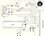
Ok Brian Thanks, that was the info I was looking for. I have attached a partial schematic that I have drawn yesterday. The author of the project connected the /CS of the flash to the PB4-/SS pin of the atmega644. He did not use any pullups, but since I now want to disable the flash temporarily, I used a pullup as you suggested and JP7 to disable the flash.

1. Do you think the pullup will cause problems to the MCU when JP7 is closed?

In the schematic you can see a simple programmer which is used to initially program the MCU with the firmware. During programming JP7 is closed so that the flash is disconnected. When the MCU is programmed, the J1, J4, J5, J6 are opened, so that the programmer is disconnected from the MCU ISP. That is the idea in general.

2. Now, can I reduce the number of jumpers in the programmer?

The way I see it is that, if no cable is connected to the DB-9 programming port:
J1 can be eliminated and the T1 left connected permanently to the ISP.
J4 can be eliminated and the D5 left connected permanently to the ISP, since I think the diode is there to prevent higher than 5v levels.
J5 can be eliminated and the line left connected permanently to the ISP.
J6 can be eliminated and the D6 left connected permanently to the ISP, since I think the diode is there to prevent higher than 5v levels.

What do you think of my points 1 and 2 above?
 

Attachments

  • Capture.JPG
    Capture.JPG
    99.6 KB · Views: 121

You are correct on all points.

However, just about every voltage in the circuit is well outside the manufacturers absolute maximum rating. It may work for someone else but they may just be very lucky, you may not be. There is a high probability of the flash being permanently damaged, possibly then taking the ATMEGA with it.

For interest only, I have a PIC based unit here that has a 9-pin D socket used for serial data and in-circuit programming. With a Pickit plugged in to it I can update the firmware and with a normal serial cable plugged in it works as a data port. In fact it normally hosts a tiny PCB inside a 'D' shell that contains an ESP8266 to allow serial over WiFi.

Brian.
 

It must have, because it works. This is not my schematic.
Noble simplicity! "It works" is an observation of limited significance. May be now but not next time. You should check if the chip allows the control signal to swing higher than Vdd + 0.6V or has built-in clamp diodes. In the latter case, Vdd will probably rise above safe limit of 3.6V.

Other cheap and dirty designs are at least providing series resistors for the control signals.

Interestingly, the Adesto AT45DB081 data sheet specifies Vcc+0.6V input voltage limit while the Atmel/Microchip version specifies absolute 6.25V. Not sure if it's a typo or actually specifying a 5V tolerant input structure. Both are however consistent regarding Vcc+0.6V limit for SO output. This means, that you need to take additional measures when operating 5V devices in the SPI bus.
 

Hi,

In my eyes J7 does not disable the FLASH, it just disconnects the pullup. This is the wrong way.

--> The pullup needs to be continously connected to the FLASH, while J7 needs to disconnect the FLASH from the microcontroller and ISP.

Klaus
 

Now I am really confused. Opinions seem not to agree.
I have built the project 2 times in different building styles and the flash always work that way.

Maybe for safety I should go the safe but idiot way, of using a big DIP switch to isolate all the flash and programmer lines completely from the ISP, so I can select between the two? I do not know, it is the simplest thing in mind that WILL work for sure.
 

Hi,

In my eyes J7 does not disable the FLASH, it just disconnects the pullup. This is the wrong way.
I should have wirtten: "In my eyes J7 in your schematic of post #12 does not disable..."
This answer refers to your schematic of post#12.

--> The schematic is wrong and needs to be corrected as explained.

No need to use multiple DIP switches. No need to change wiring of the other SPI signals.
If /CH of the FLASH is HIGH, then all outputs should be high impedance and the FLASH is disabled.

Klaus
 

Status
Not open for further replies.

Similar threads

Part and Inventory Search

Welcome to EDABoard.com

Sponsor

Back
Top