Continue to Site

Welcome to EDAboard.com

Welcome to our site! EDAboard.com is an international Electronics Discussion Forum focused on EDA software, circuits, schematics, books, theory, papers, asic, pld, 8051, DSP, Network, RF, Analog Design, PCB, Service Manuals... and a whole lot more! To participate you need to register. Registration is free. Click here to register now.

[Moved] ADC star ground and motherboard topology

Status
Not open for further replies.

SamV

Newbie level 6
Newbie level 6
Joined
Apr 5, 2014
Messages
12
Helped
0
Reputation
0
Reaction score
0
Trophy points
1
Activity points
141
Hi All,

I have an ADC layout I've been testing. The ADC board itself is a 1" square. On the ADC board I've used a star ground topology.
The ADC board connects to a motherboard with AGND and DGND between the ADC board and motherboard.

My concern is that I have the star ground on the ADC board and not the motherboard.

Is this okay? Should the star ground point be on the motherboard instead of the ADC board?

let me know if you would like any more details

Any help is appreciated
Thanks
Sam
 

My concern is that I have the star ground on the ADC board and not the motherboard? Could you give a picture?
 

My concern is that I have the star ground on the ADC board and not the motherboard? Could you give a picture?

Sure, thanks for the reply.

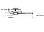
I drew a quick sketch which illustrates the ground plane connections on both the motherboard and the ADC board and how they connect to each other.
The sketch only shows the ADC, ground planes, connectors and the star ground
I've attached the sketch

Sam STAR_GROUND_CONCERN.png
 

I think the analog and digital areas have been isolated by space, without the need for AGND and DGND。
 

Hi,

sorry for the late reply, I was on vacation last week.

I think the analog and digital areas have been isolated by space, without the need for AGND and DGND。


rube,
Are you basing this on the sketch that I drew? Perhaps I should have gone with one ground plane**broken link removed**

I've attached a sketch which details where the power supply input is in relation to the ADC's analog and digital domains. The red line in the sketch shows where the split is on the ADC. (AD9230 is the converter) The pcb that the ADC is mounted on has separate digital and analog power pins as input. (They are regulated separately external to the PCB) It was a tough choice to decide whether to go with a single or split ground. In retrospect, if we had the VDDA supply input on the left side and the VDDD input on the right side, corresponding with the location of the analog and digital domains on the ADC respectively, I would have gone with a single ground plane.

Please opinions/comments wanted~

Thanks for the input
 

Page 10 of the data sheet says a common ground plane.

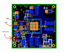
I've attached an image of one of the layers on my pcb with some hand drawn notes to help illustrate my point.
In the image all of the AGND and DGND nets are highlighted. I've drawn arrows and labeled the contacts on connector J(x) which connect to the VDDD and VDDA supply.
What I have done is pick three locations where a zero ohm resistor can be populated for star ground point. Populated a zero ohm on any of these locations shorts the AGND and DGND planes. I have also noted the location of the 'star ground' point I have chosen, near where the power supplies connect.
At this point, I believe that the motherboard which my pcb connects too will only have one ground plane seen from the perspective of my ADC.

I'm new at this high speed ( 250MHz) mixed signal layout, maybe I am trying to hard at it.
pg. 10 of data sheet:
1 AGND and DRGND should be tied to a common quiet ground plane.

I believe I have accomplished this by incorporating a 'star ground'

after reading through page 5 and 6 of this again:
https://www.analog.com/static/imported-files/tutorials/MT-031.pdf

I think it may be wise to re-evaluate this and maybe do another board spin...
I think it may be wise
STAR_GROUND_CONCERNV2.pngSTAR_GROUND_CONCERNV2.pngSTAR_GROUND_CONCERNV2.png


A common ground, that means one common ground not two.....
And if you insist on two ground you have to star them at the convertor...

"analogue and digital grounds" put this into google and read the stuff that comes up, especially Henry Ott and the Texas stuff...as well as everything else.

http://www.hottconsultants.com/techtips/split-gnd-plane.html
http://www.ti.com/lit/ml/slyp167/slyp167.pdf
http://www.analog.com/library/analogdialogue/anniversary/12.html

Thanks for your input!
I'm taking your suggestion and reading the documentation.
I've read that another common star point besides the converter is near where the power supply comes in. In any case, I have several spots in the layout to put a zero ohm resistor to make the star ground, one of them is under the converter.

I find this subject quite interesting. It seems that the general consensus is that there is a potential to create more problems then can be solved by using two ground planes.
If you notice the attached layout image of my previous post, there are arrows pointing the pins which the analog and digital supply voltages enter the board. I could not work out how the digital and analog currents could stay isolated from each other in this area and decided to use 2 ground planes.

Sam
 

Status
Not open for further replies.

Part and Inventory Search

Welcome to EDABoard.com

Sponsor

Back
Top