Continue to Site

Welcome to EDAboard.com

Welcome to our site! EDAboard.com is an international Electronics Discussion Forum focused on EDA software, circuits, schematics, books, theory, papers, asic, pld, 8051, DSP, Network, RF, Analog Design, PCB, Service Manuals... and a whole lot more! To participate you need to register. Registration is free. Click here to register now.

Mosfets to work in saturation region, but they're in Triode Region

aishakhan

Newbie level 5
Newbie level 5
Joined
Dec 6, 2023
Messages
8
Helped
0
Reputation
0
Reaction score
0
Trophy points
1
Activity points
74
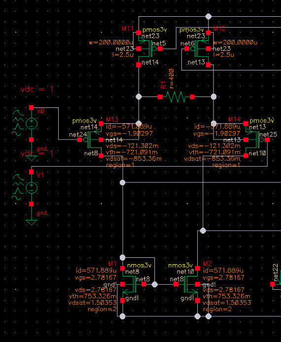
Hi, I'm new here and also I'm new to Analog IC Design, actually I'm implementing an IA design which was in 350nm technology node, and I'm implementing it in 180nm. I'm having this issue that the MOSFETS need to operate in sat region, but they're operating in triode region. Could anyone tell me what to do so that my mosfets all work in the saturation region? Here's an attached image of the design: M11, M12, M13, and M14 all are in triode region, and I need it to be operating in saturation region. Any help would be really appreciated. Regards.
1702887867930.png
 
(1) Not -all- transistors under all conditions can be in saturation.
Pick your battles.

(2) Fold your cascodes, if they aren't already

(3) Go to a rail-rail input design, as you're not going to want to
throw away half of your common mode input range.

(4) Basic: keep L for Rout, use low-VT devices if available (not
zero-VT). Then same W ought to give you about 2X ID for Vgs
on same-ish-VT and you'd be further toward saturation from
the start. Unless your bias is whack.
 
Quotation feature of the forum does not work for the the moment. Anyway.
W/L ratio does not identify directly the operating region because since the conditions above are satisfied, the transistor enters into saturation mode independently of W/L ratio.
Here the trick is to choose the right current and the right bias ( Vgs) for MOS transistors.
For instance M1 and M2 MOS transistors sink the necessary voltage headroom for PMOS pair. Vds=2.76V !!
Normally these transistors should have Vds=0.xx ( approx) Volt. Because they are current mirror and Vgs voltages should be close or a bit higher than Vds.
There must be either an applet or small calculator in order to find W and L dimensions for each process.
 
If you are new to Analog IC design, I would suggest that you start with a simpler design such as a current mirror so that you can understand the process and not be tinkering around. Jumping directly into porting a design might not be the right path.

"Could anyone tell me what to do so that my mosfets all work in the saturation region?"

"Yes you're right, but how will I choose different values of W/L so i get them in saturation region? Is it like a hit or miss situation, like randomly selecting different Widths and lengths and simulating them? "

The answer to this would be "Design the Mosfets so that they are in the region you want them to be in." Simply tinkering around with the sizes will do you no good.
You are using W and L sizes that were designed for a totally different process where obviously the Kn/Kp, Cox etc are different than what you have now.

I would suggest that you start by designing a current mirror PMOS and NMOS with the similar current as your amplifier. See what it takes to design it such that the transistors in the mirror are in the correct regions and then use that information in your amplifier design.
 

LaTeX Commands Quick-Menu:

Part and Inventory Search

Welcome to EDABoard.com

Sponsor

Back
Top