Continue to Site

Welcome to EDAboard.com

Welcome to our site! EDAboard.com is an international Electronics Discussion Forum focused on EDA software, circuits, schematics, books, theory, papers, asic, pld, 8051, DSP, Network, RF, Analog Design, PCB, Service Manuals... and a whole lot more! To participate you need to register. Registration is free. Click here to register now.

MOSFETs connected in series

Status
Not open for further replies.

komax

Junior Member level 3
Joined
Dec 2, 2019
Messages
31
Helped
0
Reputation
0
Reaction score
0
Trophy points
6
Activity points
312
Let's say I have 5 NMOS with size W/L connected in series (stacked) with gate connected together, from what I understand this is functionally equivalent to a single NMOS with size W/5L.
In terms of saturation check only the top NMOS will be in saturation while the other 4 will be in triode. My question is regarding this saturation check, specifically when checking Vgs - Vth > 100mV for achieving strong inversion. The Vgs in that equation, is this the Vgs of the top NMOS or the bottom?

I'm thinking that it's the bottom NMOS, my logic is as follow: Suppose the gate voltage is Vb (wrt ground), if I have a single transistor with size W/5L my Vgs will simply be Vb, and since my stacked transistor is supposed to be equivalent if I take the Vgs of the top transistor my Vgs will no longer be Vb. If I take the Vgs of the top NMOS it is much harder to maintain strong inversion, this is especially so the more I stack the NMOS because the Vgs will simply be Vb - Vx (v at source) and Vx is getting higher and higher as I stack more. This isn't the case if I use single transistor with W/5L, W/10L, W/20L, my Vgs stays Vb (to ground).

Please help me understand.

Thank you in advance for your help.
 

not familiar with W/L, but i do know a little about driving FETs

Let's say I have 5 NMOS with size W/L connected in series (stacked) with gate connected together,

please provide a sketch showing all 5 devices, how they are wired, and how Vgs is applied to each

to turn the devices on, you need to provide Vgs > (a few volts)
if all of the gates are tied together, how are you applying Vgs to each device?
 

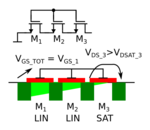
Here is the sketch: link

I only drew 3 devices but conceptually they are the same. Basically NMOS connected in series.

The top most transistor will be in saturation and the other 4 will be in triode.
 

i have never seen that configuration
please provide a reference that describes its operation

simple, first round view of behavior:
i can see this acting like a switch.
if Vds is small, then Vgs can be big for all three FETs

when it is off, i would expect a voltage balancing resistor across ds of each FET
so each FET sees the same voltage across ds

when it is turning on, i think the bottom FET turns on first
then the middle FET, then the top FET, as each FET sees a Vgs big enough to turn on
they do not turn on all at once
the voltage across the off FETs will step up as each FET turns on
off - 1/3 voltage each
one on - 1/2 voltage each remaining
two on - full voltage on one.
if one FET could hold off the voltage, you would not need 3 (or more) so this destroys the FETs

if it is operating in the linear region, it will take more time and thought than i have time for now

as i said, please provide a reference and explanation so i can be educated
 

Playing with W/L is only feasible in IC design. In regular NMOS or CMOS technology, you have a common substrate for all NMOS transistors, hence the assumption of different Vgb for stacked transistors with common gate connection is incorrect. If you abstract from drain and source contact effects, five stacked transistors of size W/L behave like a single W/5L transistor in the first order.
 

@wwfeldman, Thanks for the reply, sorry I don't have reference explanation for you, I'm looking for information myself.

- - - Updated - - -

Playing with W/L is only feasible in IC design. In regular NMOS or CMOS technology, you have a common substrate for all NMOS transistors, hence the assumption of different Vgb for stacked transistors with common gate connection is incorrect. If you abstract from drain and source contact effects, five stacked transistors of size W/L behave like a single W/5L transistor in the first order.

Thanks for the reply.
Indeed I am referring to IC design, analog ICD specifically. To check transistor strong inversion, do you think I should check the top or bottom NMOS?
 

Look on attached figure. I hope it should dispel your doubts.
stackd_fet.png
 
  • Like
Reactions: komax

    komax

    Points: 2
    Helpful Answer Positive Rating
As you have already said, only the top transistor is in saturation, the rest towards ground are in linear with the bottom one most strongly in linear. Your question is how to define Vgs and which Vgs to take into account. I will rephrase it as finding the overdrive voltage Vov, which is something you want to know if using that stacked transistors in analog design. I can offer you a kind of approximate answer to that. Today's transistors don't really behave like square low devices so exact formula will be difficult to come up with. Suppose you have one NMOS with W/L. You are mostly interested in the overdrive voltage Vov, which in square low speak is 2/(gm/Id), so actually for saturation you want to know gm/Id. Simplistically, for the same current and W/L, if transistor is in triode region its Ron=1/gm (gm being the gm when it is in saturation).
Now, if you put two of these transistors in series with the same gate voltage, the top one will be in saturation, the bottom one in triode. The Vov of the top NMOS is 2/(gm/Id) and the voltage drop across the bottom one is Ron*Id=1/(gm/Id). So, the "overdrive voltage" of the combined two transistor stack is 3/(gm/Id). If you have 3 transistors in series, you get something like 4/(gm/Id) and you can extrapolate further. You need to size the transistors such that the gm of the top one gives you the equivalent Vov that you need.
As I said, this is not exact. However, if you simulate the Id vs. the drain voltage of the top device (kind of the equivalent Vds of the stack) you can see that the equivalent transistor goes into saturation at about approximately (quite approximately but not terribly too much) that Vov.
If you want to share your simulation results here, it will be interesting to see what you get.
 
Last edited:

Thank you for the reply @Dominik, much appreciated.

- - - Updated - - -

Thanks @sutapanaki for the explanation
 

Status
Not open for further replies.

Part and Inventory Search

Welcome to EDABoard.com

Sponsor

Back
Top