Continue to Site

Welcome to EDAboard.com

Welcome to our site! EDAboard.com is an international Electronics Discussion Forum focused on EDA software, circuits, schematics, books, theory, papers, asic, pld, 8051, DSP, Network, RF, Analog Design, PCB, Service Manuals... and a whole lot more! To participate you need to register. Registration is free. Click here to register now.

MOSFET switching MSP430

Status
Not open for further replies.

yassin.kraouch

Advanced Member level 2
Joined
Jul 5, 2009
Messages
631
Helped
40
Reputation
80
Reaction score
40
Trophy points
1,308
Activity points
5,094
Hi,

i have to design a switching circuit using a msp430, the MOSFET used is

https://www.fairchildsemi.com/ds/FD/FDS9926A.pdf

the microcontroller is https://focus.ti.com/lit/ds/symlink/msp430f133.pdf

i have a trouble in choosing the MSP430 ? can the msp430 be used to switch on/off the MOSFET ? is there any condition in current ??

can i drive 6 mosfet gate using one single PIN that generate PWM, or i should use 6 pin from the MSP430 that generate PWM for each gate ?

please i need help asap
 

If you check page 28 of the datasheet (mcu) it has the graphs that show the output voltage vs output current.
The current you can get is a few mA, if the mosfets are going to be use as switches (to control on/off) then there is no problem but for high speed PWM you need a proper high current driver for fast turn on/off of the mosfets and low heat losses.

Alex
 
thank you alexan_e for the reply, for what frequency the current will cause a problem ?
 

The MOSFET datasheets have a very important factor called Total Gate Charge and is given in nC.
It is actually the time * current at which the MOSFET is fully on, for example when you read 100nC it means that if you give 1A (limit the gate current to 1A is what i mean) the gate will be charged after 100ns (100nC /1A = 100ns ) or if you give 10mA the gate will be charged after 10000ns (100nC /0.01A = 10000ns ) etc
So when you choose a MOSFET and driver you should consider the parameters for both of them (MOSFET with lower nC are faster)
For mode details you can read
https://www.fairchildsemi.com/an/AN/AN-9010.pdf
see page 17 for the different gate capacitance charge stages

Once the mosfet is conducting , when you want to turn it off you need to discharged the gate capacitor, the faster you discharge it the faster it will turn off.
In simple switch application you may just stop driving the gate but when you are using a high frequency and you care about the speed you have to use a push pull circuit to give or pull current fast.
In addition when a mosfet is neither on or off and is in the between stage it gets hot because of the current multiplied with the voltage drop across the source-drain, when it is off you have no current and when it s on you have very small voltage drop (because of low on resistance).

I don't think you gen get away with a few mA drive for PWM switchin even if it is 1KHz, you will have heat problems and low efficiency.

Alex

---------- Post added at 13:25 ---------- Previous post was at 13:14 ----------

Also check this
**broken link removed**

Alex
 

i have another problem, is there any microcontroller that can resolve this problem, i think low power mcu does not resolve the proble
 

I don't know of any mcu that can provide a current that is high enough to drive directly a fast switching mosfet.
You either need a proper mosfet driver chip , like for example **broken link removed**

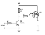
or you can make a discrete driver that will give much better speed than an mcu can, like for example
Nmosfet_drive.gif
it will provide about 50mA or more depending on the resistor and supply voltage.
The turn off current is controlled through the 220 ohm resistor and turn on gives the max that the transistor can based on the base resistor and current gain

or you can go for the full totem pole driver which would give the best result
N-Mosfet_driver.jpg
it can sink/source about 2-3 Amperes

Alex
 

but alexan_e if you see in the datasheet of the mosfet, this transistor support TTL/CMOS level, and have a small charge Q=9ns, what do you think if the frequency swith is 20 KHz ? i think that this will not cause problem ?
 

You can try it to see if you will have heat problems on the mosfets.
First of all you are using a 3.3v mcu, assuming that you want to drive the mosfet to 2.5v (as specified in the datsheet for 43m ohm) you have to use a resistor and limit the current to about 7mA (mcu datasheet).
The best case scenario is to drive a single mosfet with that 7mA, the total gate charge in low but I'm still not sure that it can work properly.
The TTL level describes the voltage level in which the mosfet can work properly (turn on and have a low Rds-on), it is based on the gate threshold voltage , not on the gate charge rating.

Alex

---------- Post added at 17:35 ---------- Previous post was at 16:57 ----------

If you do a calculation for the total gate charge of 9nC

9nC/0.007A =13us to turn on and 13us to turn off

with a 20kHz PWM you have a period of 1/20000=50us , the switching rate is half of that because you have 25us high / 25us low assuming 50% duty, it is already faster than the calculated speed (13+13us=26us min width).

If you go at a higher or lower duty ratio for example 20% then you will have 10uS on / 40us off which is a speed in which the mosfet will not be able to work.

Alex
 

insert a resistor will slow the gate charging process, to solve this problem i will use a capacitor in parallel to this resistor, chat do you think about this idea ? and what is the value to choose in order to limit the current ? and also the capacitor ?
 

The resistor has to be inserted between the mcu and gate to limit the current pulled from the mcu (to the mosfet), this will protect the mcu and keep the voltage output above a minimum level (2.5v).
If you don't use a resistor then you stress the output stage of your mcu and you will also get output voltage close to zero because of the internal voltage drop (the high output becomes 0v with just 25mA of current)
The point of the resistor is to limit the current, if you are going to bypass it then don't use it in the first place.
The resistance value is a good question, I have no idea how to calculate it because the output voltage is not constant and you will also get a voltage drop on the resistor.

Alex

---------- Post added at 19:11 ---------- Previous post was at 18:47 ----------

I'm nor sure about the external resistance.
The internal resistance is so high (based) on the graph that will limit the current anyway to a max of 25mA but the problem is that you don't want the output voltage to go below 2.5v (which is at 7mA) and I have no idea how to accomplish that.

Alex
 
Last edited:

Status
Not open for further replies.

Similar threads

Part and Inventory Search

Welcome to EDABoard.com

Sponsor

Back
Top