Continue to Site

Welcome to EDAboard.com

Welcome to our site! EDAboard.com is an international Electronics Discussion Forum focused on EDA software, circuits, schematics, books, theory, papers, asic, pld, 8051, DSP, Network, RF, Analog Design, PCB, Service Manuals... and a whole lot more! To participate you need to register. Registration is free. Click here to register now.

Mosfet rise curve in deep.

DM0119

Junior Member level 1
Joined
Feb 24, 2019
Messages
16
Helped
0
Reputation
0
Reaction score
11
Trophy points
3
Activity points
103
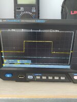
Is this curve of the rise in a mosfet,acceptable to work in a H bridge?
Something stops the rise for 40ns at about 4,5 volts.
What should be causing this phenomenon?

IMG_20240710_133435.jpg
 
You should say you are showing the G-S waveforms - not every one on here is a mind reader

the plateau is where the V ds is falling and pulling current out through Cdg holding the gate flat when it would other wise be rising

a similar but opposite thing happens at turn off

this is basic power electronics for newbies - I mean really basic stuff - mosfets have ( often variable with voltage ) capacitance between all 3 terminals - and this affects switching behaviour.
 
The flat spot is where the MOSFET reaches its Vgs(th) value and starts to turn on/off, so then the Miller capacitance kicks in and pulls charge from the gate to the drain.

Below is the LTspice sim of a simple MOSFET switching circuit, showing this relationship between the gate voltage through a 20Ω source resistance (yellow trace), the gate charge current (blue trace) and the output voltage (red trace):
Once the the output switching is finished, there's no more Miller capacitance current, and the gate voltage then continues its rise/fall.

1721005119632.png
 
Actually - for completeness - the mosfet picks up all the current just at the very sharply rising slope and minor blip at the start of the plateau - for inductive switching - any switch mode psu - the voltage cannot begin to fall until the mosfet has picked up all the current - and the plateau effect relies on falling Vds

so you see - current rise time first - which you cannot really see - unless you look really hard at Vds ( a very slight dip before falling ) - then voltage fall time, second.

Proper data sheets when referring to switching time - e.g. turn on - refer to current turn on time, ditto turn off, turn on time is not really related to Vds fall and vice versa - however mosfet losses are strongly related - esp if the volt fall time is overly long.
 
Lots of other ap notes on web and gate charge considerations.

Attached :


Regards, Dana.
 

Attachments

  • Infineon-Gate_drive_for_power_MOSFETs_in_switchtin_applications-ApplicationNotes-v01_00-EN.pdf
    1.6 MB · Views: 174
Thank you very much for your answers.
I clearly understand all the things that you very well explain to me about this.
You ensured to me all my thoughts about it.

So, Is this something will can cause damage to the device?This is the signal looks like.
 

Attachments

  • IMG_20240712_121223.jpg
    IMG_20240712_121223.jpg
    1.2 MB · Views: 89
Last edited:
One primary concern with H Bridge is to insure you have dead band timing,
to insure both MOSFETS in vertical leg never on at same time :

1721044459891.png


Regards, Dana.
 
"Easy peasy.The voltage drops actually is almost nothing for the gate,i would say we have voltage stop ,not drop.
The time this happens is at 40 ns.Therise time is a bit lower than 200 ns the falls is a bit lower than 160 ns.
 
One primary concern with H Bridge is to insure...

Dead time is at 1μs for testing.Rise time is a bit lower than 200 ns,fall time is a bit lower than 150ns. For the high side.
Low sided is at almost same times with a slight deference.
 
Last edited by a moderator:
A significant concern is the transistor switching dissipated power which equals the energy dissipated during the rise/fall time times the frequency of the switching.
This is added to the ON dissipation determined by the MOSFET on-resistance and current load.
That affects the efficiency of the circuit and whether a transistor heat-sink is needed.
 
Η επόμενη ερώτηση μου έρχεται αυτόματα και είναι:
Μπορεί αυτό να βελτιωθεί με έναν πολύ μεγαλύτερο ενισχυτή για οδήγηση; Τώρα χρησιμοποιώ αυτό που περιγράφεται στη συνημμένη φωτογραφία. Είναι περίπου 7 αμπέρ ενισχυτής.

Screenshot_2024-07-08-23-19-56-951_com.miui.gallery.jpg
 
The time spent in the Miller plateau is the width of the
dissipated-energy-thermal-pulse in the core of the FET
and the largest chunk of switching loss (absent any FU
in the drive phasing). If you're turning on into an existing
circulating current this can be substantial (high Id, medium
Vds hanging out).

Hard turnon switching optimizes efficiency but worsens
EMI. HL output switching has a sweet spot between too slow
(current onto back-diode) and too fast (cross conduction)
which needs a timing servo for across-the-envelope optimization.
 
for inductive switching - any switch mode psu - the voltage cannot begin to fall until the mosfet has picked up all the current - and the plateau effect relies on falling Vds
Yes this is true...and you can play with it...because the FET doesnt "know" what the current should end up being...so what you do with eg a hard switched forward or bridge SMPS, is you make a non_sandwich_wound transformer, so that you have reasonably high leakage inductance...and then this leakage L will slow up the rise of current in the fet when it turns on....and you end up traversing the entire VDS without having to conduct the full "ultimate" current whilst you do so...so your turn-on switching losses are much lower.

So your Leakage L works as a turn on snubber for you.
 
Thanks all of you for your answers!

All understood!


One last thing I would like you to tell me based on your experience, if this pulse is acceptable to work safely in spwm Low frequency transformer inverter.

(Up and down leg complementary pulses 24 khz.)

MOSFET:fdh055n15
We need 40 amps.
Supply Voltage 45-60.


The dead time logically according to the switching times will be set to 500ns.


1) Do I leave him as he is?

2) do I delay switching?

3) Speed up switching?
 
Its a plain Full Bridge SMPS?
As long as the FET is defiNitely off before the next one turns on then youre OK.
Whats you max duty cycle....?...the fet neednt be on any longer than that suggests, so you can use that to set dead time if you want.
 
Spwm full bridge inverter.
Max duty cycle at 71% (sinusoidal pulses).
Sw Freq 24 kHz.
45-60 V supply.
40 amps.
Fet is: fdh055n15a.
Output voltage 230.
 
The next question that comes to me automatically is:

Can this be improved with a much larger driver amplifier? Now I use the one described in the attached photo. It's about a 7 amp amplifier.

Screenshot_2024-07-08-23-19-56-951_com.miui.gallery.jpg
 
Some of your images are just black spaces - - your gate drive is just good enough to drive the fets in the inverter you describe - good luck and don't forget to use generous heat-sinking on your fets !
--- Updated ---

"Easy peasy.The voltage drops actually is almost nothing for the gate,i would say we have voltage stop ,not drop.
The time this happens is at 40 ns.Therise time is a bit lower than 200 ns the falls is a bit lower than 160 ns.

That's because you are looking at it without power on a real circuit - post a clear image again when the fet is doing real work !
--- Updated ---

Also there are plenty of gate drive solutions if your present gate drive proves to be too weak

- a standard emitter follower npn pnp

- a high and low side GD chip with boot strapping diodes for the upper power - buffered with emitter follower
 
Last edited:

LaTeX Commands Quick-Menu:

Similar threads

Part and Inventory Search

Welcome to EDABoard.com

Sponsor

Back
Top