Continue to Site

Welcome to EDAboard.com

Welcome to our site! EDAboard.com is an international Electronics Discussion Forum focused on EDA software, circuits, schematics, books, theory, papers, asic, pld, 8051, DSP, Network, RF, Analog Design, PCB, Service Manuals... and a whole lot more! To participate you need to register. Registration is free. Click here to register now.

MOSFET as Load switch

Status
Not open for further replies.

suryakant

Member level 5
Member level 5
Joined
Mar 10, 2005
Messages
90
Helped
6
Reputation
12
Reaction score
0
Trophy points
1,286
Location
India
Activity points
2,171
mosfet load switch

Hi all,
I am using MOSFET to switch on/off supply to one section of my circuit. Supply voltage is 3.3V

The circuit is attached here.
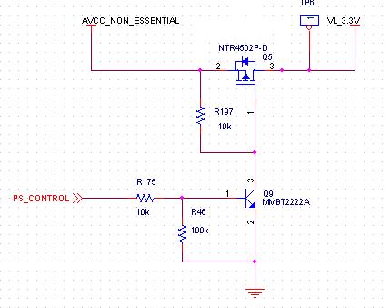
85_1237464815.jpg


When PS_Control is HIGH, I get 3.3V.
But, when PS_Control is low, still I am getting approximately 1V at the output. But i want the voltage to be zero. Whats the reason for this? Do I need to modify the circuit?

Thanks.
 

load switch

When the MOSFET is OFF Test-Point VL_3.3V is floating .. and you have a tiny leakage current ..
Try to add a "dummy" load of, say, 100kΩ that will pull the voltage down to 0V ..

Rgds,
IanP
 
mosfet as a switch

Hi IanP,

Actually load is 2 op-amps LMV324. I also tried to put dummy load, but no help!!!
Its still at about 1V.

But if I replace BJT by N channel MOSFET, it works fine......

I am just wondering what would be the reason.
 

mosfet switch

Either the real circuit is different from your schematics, PS_CONTROL is above 0.6V in low state or the transistor is defective.
 

Re: mosfet as a switch

Hi IanP,

Actually load is 2 op-amps LMV324. I also tried to put dummy load, but no help!!!
Its still at about 1V.

But if I replace BJT by N channel MOSFET, it works fine......

I am just wondering what would be the reason.

Hi Suryakant,

can you put the schematic with thr BJT replaced with n-channel Mosfet?
Thank you a lot, Antonio
 

Unlike bipolar transistors, power MOSFETs have a considerable
gate capacitance that must be charged beyond the threshold
voltage, VGS(TH)
, to achieve turn-on. The gate driver must provide
a high enough output current to charge the equivalent gate capacitance, CEI
, within the time required by the system design.

https://ww1.microchip.com/downloads/en/AppNotes/00786a.pdf
 

Status
Not open for further replies.

Similar threads

Part and Inventory Search

Welcome to EDABoard.com

Sponsor

Back
Top