joujou
Junior Member level 3

Hi to all,
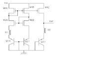
I am interested in modeling (setting equation) the PSRR of a Bandgap circuit shown below. This why,we must make the equivalent small signal schematic of this circuit and then we express the gain between a signal at Vcc and the output of the BG.

The problems:
1) Does the lateral parasite PNP transistor used is modeled by a dynamic resistance Rd
2) Is there a volunteer who can help me to make this schematic and then set the gain Vref / Vdc
I am interested in modeling (setting equation) the PSRR of a Bandgap circuit shown below. This why,we must make the equivalent small signal schematic of this circuit and then we express the gain between a signal at Vcc and the output of the BG.

The problems:
1) Does the lateral parasite PNP transistor used is modeled by a dynamic resistance Rd
2) Is there a volunteer who can help me to make this schematic and then set the gain Vref / Vdc