Continue to Site

Welcome to EDAboard.com

Welcome to our site! EDAboard.com is an international Electronics Discussion Forum focused on EDA software, circuits, schematics, books, theory, papers, asic, pld, 8051, DSP, Network, RF, Analog Design, PCB, Service Manuals... and a whole lot more! To participate you need to register. Registration is free. Click here to register now.

Mentor Graphics Net Properties

Status
Not open for further replies.

vikash23

Full Member level 2
Full Member level 2
Joined
Jul 31, 2012
Messages
133
Helped
3
Reputation
6
Reaction score
3
Trophy points
1,298
Activity points
2,676
Hi,

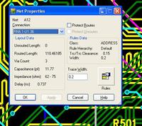
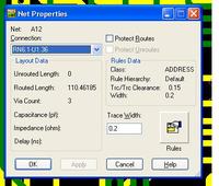
I have attached two images. One is my old PCB layout and other one is new PCB layout. I was not able to look at capacitance, impedance, delay in my new layout. The changes that i have made in my new PCB compared to old is layer stack up and increased layer from 6 to 8.

Can any one please help me how to figure out this ?
 

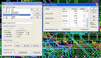
Have you defined your layers? thickness, dielectric etc.?
 

Hi Barry,

I am sorry, Can I please know where do I need to define that ?

- - - Updated - - -

Can I please know if this is what you are saying about ?


Yes, that's what I was talking about. But you might also have to make changes under Tools/VerifyDesign check High Speed, click Setup, Parameters. There might be something in that area that's not configured properly.
 
  • Like
Reactions: vikash23

    V

    Points: 2
    Helpful Answer Positive Rating

    vikash23

    Points: 2
    Helpful Answer Positive Rating
Thank you,

My next question is will the layer stack up change and increase in number of layers will affect the delay, impedance and capacitance of a signal even though both the revisions of the PCB has got same track length and width ?

I compared the delay, impedance and capacitance for a same signal on both the PCB's. I found it to be different. Previous revision of the PCB works fine but not the new revision.
 

Of course. The impedance, etc. is directly related to the dimensions of your stackup.

But back up a minute. What do you mean 'previous revision of the PCB works fine but not the new revision."??? If the new board doesn't work, I'd be looking at things other than impedance; like maybe a layout error. What is it that "doesn't work"?
 

The data and address line connecting between RAM and DSP are of same length , width in both the revisions of the PCB. Previous revision of the PCB stack up is as follows

Top
3V3(Cam Plane)
Inner Layer 3
Inner Layer 4
DGND
Bottom


New revision of the PCB stack up is as follows

Top
DGND-1
Signal-1
Power-1V4
DGND-2
Signal-2
Power-3V3
Bottom
.

But from the software team gave feedback as the new PCB doesn't seams to work like the previous one and they say they were not able to control the address and data signals.
 

You are not giving us a lot to go on. "Not able to control the address" doesn't mean anything. Do you mean that the DSP is not driving the lines? Is there a timing issue? Is there a short? Have you looked it the signals with an oscilloscope?
 

I am in a basic level in electronics. So that is the reason why I was not able give you a lot to go on. I dint involve much in this DSP problem.

I haven't tried looking at the signals in the oscilloscope.

Once I get a clear idea of the problem I will come back to you.

Thank you for your help Barry.
 

Status
Not open for further replies.

Part and Inventory Search

Welcome to EDABoard.com

Sponsor

Back
Top