Continue to Site

Welcome to EDAboard.com

Welcome to our site! EDAboard.com is an international Electronics Discussion Forum focused on EDA software, circuits, schematics, books, theory, papers, asic, pld, 8051, DSP, Network, RF, Analog Design, PCB, Service Manuals... and a whole lot more! To participate you need to register. Registration is free. Click here to register now.

Memory Banks

LakshmiJL

Junior Member level 2
Joined
Oct 7, 2014
Messages
20
Helped
0
Reputation
0
Reaction score
0
Trophy points
1,281
Activity points
1,413
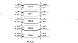
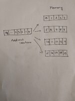
I need to divide a memory into multiple memory banks(more than 2) and write data to each of the memory bank simultaneously. In this case how is the write and read operation managed. Should I have same number of read and write ports as that of the memory bank?Thanks in advance
 
Assuming this is dual-port memory, just tie all your input data lines and enables together so it will look like one write port. Obviously, you have to have separate read ports.

But, I have to ask, if you're writing the exact same data to multiple memories, what's the point? No matter which memory you read, it will be the same, right?
Thanks for your reply.The data is not same. They are different data. For example of if I have 20 data, instead of writing serially into memory, I am thinking of dividing the memory into banks and writing and reading them parallely. For example 4 memory banks for 20 data,5 data parallely written in each.So latency can be reduced.
 
Draw a picture. Are you saying you want to write 20 bits as 5 bit chunks into 4 5-bit wide memories? Why is that any different than writing 20 bits into a single 20-bit wide memory?
 
Draw a picture. Are you saying you want to write 20 bits as 5 bit chunks into 4 5-bit wide memories? Why is that any different than writing 20 bits into a single 20-bit wide memory?
If i have data in 20 address locations, I would need to write data from it parallely into memory banks like below.
 

Attachments

  • Memory_bank.png
    Memory_bank.png
    46.8 KB · Views: 8
  • Memory.jpeg
    Memory.jpeg
    65.2 KB · Views: 8
It still is unclear.

The sketch shows one address line and one data line per RAM.
Usually one has address lines to access 2^n different locations.

And usually a RAM has a counterpart to communicate with. A microcontroller an memory controller or it may be some FPGA internal logic.
In either case it should have a defined address bus, data bus, control signals.

What you call RAM seems to be a single data flip flop. Is this the case?

Please give more details about your real application... not some fictive example.

Klaus
 
If i have data in 20 address locations, I would need to write data from it parallely into memory banks like below.
Means that the source ("20 address locations") can't be FPGA block RAM, because block RAM has maximal two ports that be operated simultaneously.
 

LaTeX Commands Quick-Menu:

Part and Inventory Search

Welcome to EDABoard.com

Sponsor

Back
Top