Continue to Site

Welcome to EDAboard.com

Welcome to our site! EDAboard.com is an international Electronics Discussion Forum focused on EDA software, circuits, schematics, books, theory, papers, asic, pld, 8051, DSP, Network, RF, Analog Design, PCB, Service Manuals... and a whole lot more! To participate you need to register. Registration is free. Click here to register now.

Matching circuit for RF energy harvester

Max077

Newbie level 5
Newbie level 5
Joined
May 13, 2024
Messages
9
Helped
0
Reputation
0
Reaction score
0
Trophy points
1
Activity points
76
Hello,

I want to design a matching circuit using ADS for RF energy harvester between antenna and rectifier.
The antenna impedance is 50 ohms. How can I calculate the impedance of the rectifier circuit?

I would like to use the smithchart for matching but I am stuck in rectifier`s impedance.
I have read it can be calculated through HB analysis but I am not cleat how exactly I can?

Thank you.
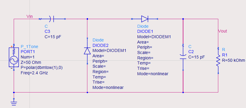
Screenshot 2024-05-13 164451.png
 
Search forum quoting as " RF Rectifier" "RF Harvesting" " ADS Rectifier Circuit" etc. You'll find many useful information about them.
We discussed this subject deeply in many times.
 
Impedance matching is supposed to maximize power throughput. Incoming voltage & current may be at levels not usable by your following circuitry. Therefore the aim (when harvesting RF energy) is usually to raise volt amplitude even though it means current must be reduced in the same fashion. By doing that power throughput is maximized, because voltage & current levels are optimized for your following circuitry.

To get any signal (power) through your circuitry, its volt level must overcome the diode threshold. Your schamatic is a Villard voltage doubler. You would need several such charge-pump stages in order to impedance match 50 ohm incoming to 50k outgoing. With so many such stages you'd lose power instead of maximizing power.

Some kind of LC arrangement is better able to match impedances in this case.
I would like to go for 2 stages to get the desired voltage but before going forward I need an impedance matching between antenna and rectifier. I understand matching can be achieved through LC or TL based but I need to find the impedance of the rectifier, how can I find the impedance of the rectifier?
 
A diode alter's its internal impedance depending on applied voltage and current. The result obeys a formula which can be approximated as:

A=(V x 1.25) ^ 21.

So when it's conducting 1A, expect it to read 0.8V. I took several readings of a silicon diode, how much voltage causes so much current. I graphed the results. I saw that the diode starts to conduct a small amount around .4 V. Fitting an equation to the graph took me a lot of testing. Of course the complicated Shockley equation for diodes. takes a few more parameters into account.
 
Hi,
You can use LSSP and HB and Zin analysis to measure rectifier's input impedance at a given frequency and input power. Run these analysis and then set the source impedance to be the conjugate of the measured Zin, repeat this process again until you get a good matching result shown on the S11 graph at the input frequency, That is the final input impedance.

Here it is explained very well in details with pics.

Alothman, Abdullah. (2021). Re: How to calculate Impedance of diode in rectenna design?. Retrieved from: https://www.researchgate.net/post/How_to_calculate_Impedance_of_diode_in_rectenna_design
 
Last I looked at this was a couple of decades back
for RFID tags, at RX power levels you will lose all
the energy just trying to climb that front diode's
I-V curve and fall back. A charge pump is not the
same thing as a detector, and you are looking to
pull energy from as close to zero amplitude as possible
(because your customers want range and don't want
to humor you about specific placement of -their- stuff).

The only thing that came close to working for me was
a high-Q antenna tank that would "ring up" to an
amplitude that let low-VT / intrinsic MOS diodes do
a little rectifying at the crest. Didn't work well enough
to sell the job, so I never did get any smarter (only
smart enough to stay away from future RFID stuff
in favor of things I was good at).

I am pretty sure you want nothing to do with an
ohmic antenna-match. Frequency-match to the tank
with non-lossy components.
 
Consider what you wish to build is similar to the old-fashioned 'crystal' radio set. Needs no power to run. Takes its power out of the air from radio broadcast waves. Your aim is to gain maximum strength of voltage and current, whatever techniques you might find to use. Often it's a long antenna, that is, a long wire designed to receive the transmitting frequency, and a resonant circuit designed to assist reception.
 
If you want to measure the impedance of the circuit under HB you will need to add a current probe before C3.
In post processing you will need to calculate Zin = Vin/Iin.i
Then calculate gamma from Zin to plot on smith chart.
Make sure you have enough harmonics in HB controller, maybe 8-10 (assuming model is still valid at really high frequency).
The diode is dynamic so needs to be either HB or TRAN simulation with enough power applied.
 
Hi,
You can use LSSP and HB and Zin analysis to measure rectifier's input impedance at a given frequency and input power. Run these analysis and then set the source impedance to be the conjugate of the measured Zin, repeat this process again until you get a good matching result shown on the S11 graph at the input frequency, That is the final input impedance.

Here it is explained very well in details with pics.

Alothman, Abdullah. (2021). Re: How to calculate Impedance of diode in rectenna design?. Retrieved from: https://www.researchgate.net/post/How_to_calculate_Impedance_of_diode_in_rectenna_design
Any f domain analysis only with a diode which changes impedance in time over the entire cycle is invalid. Also considering the level 0 model in the ELF range is also invalid for 2.4GHz.

To capture this signal, one must amplify with a lossless resonator which will be difficult to exceed useful power levels for any diode. This Q amplification raises both V and Z for the load. Good ruck. parasitic C of the diode is also nonlinear.
 
Any f domain analysis only with a diode which changes impedance in time over the entire cycle is invalid. Also considering the level 0 model in the ELF range is also invalid for 2.4GHz.
That's why the classical ADS "rectenna" homework exercise uses HB (harmonic balance) analysis and realistic microwave capable diode models. Learning objective of the exercise is to practice this analysis method, not to reinvent the wheel.
 
The rectifier matters, a lot.

Old true crystal radios used galena (PbS, a natural II-VI semiconductor) as a point-contact Schottky diode of low Vf and low shunt-C.

In the '70s I had one of those "spy pen radios" from the back of a magazine. Probably a germanium diode there, silicon costs you twice the Vf before you harvest / demodulate a thing. You got antenna input power to spare? Yeah.
 
One can approximate the impedance of any sw
That's why the classical ADS "rectenna" homework exercise uses HB (harmonic balance) analysis and realistic microwave capable diode models. Learning objective of the exercise is to practice this analysis method, not to reinvent the wheel.
I've not done that method, yet I know the efficiency and impedance of the model changes with input power or e-field or flux level. The diode has an effective duty factor on conductance with fixed L and variable R(I), C(V). Thus one must be aware of the assumptions.

This may add intel to the topic https://scholarbank.nus.edu.sg/bitstream/10635/53657/1/SunHC.pdf?termsofuse=on&usertype=Public&usertype-input=&institution=N/a&research=&g-recaptcha-response=03AFcWeA5YJan4Lbp5skghlQFBUpupgf6xfheJ5WeW_IGa3wObOOZlpkr_6BRWp6ynV6SmsvrwGtOYZKBcPsNFw2tp-q4PSVGttA1Yi9EBAW9R_ZXNb6mh__zROXEWm4zevWlOmBhtmnW4rXGYVuOm1TjBd35AXvuruNqB-GKK4BRD9Oq_n6Qv47WmcKTlFMq5HH9FFHxEHoUjZTKligItt_a49OgZT58Ig7ZDLJpQ17J5HLtlhyJCrDMNPpjyi5jxdhEV7tzTBC9Yd4q7kKm_4SZm89nS2TGh5IhHbAyLzCvZZhLO12FGQKCSEJrVFAYlbHZzvsCldl7sCBYHEIcATcHK_zc9ssqYQZVMsqcbaGONLDRQdvUqcSGrKbMZmfo_ioQSe5MoYmrTQkZq-WaTXNJ1DDso0GawNAcOf8DP9Ct9yUIE-aDYOT9Pk9i21GUqmfZSS7_czZIdZIyyraFI16PFsDA090jnIL1S9WCfE6SzgXC6-y8t1BnbqRtNMp3WSQMj1ZPQn3IXRUxRMSgj0Z0VUdL2IHK6AxPMqPvqTuoGkTt4iu56eEce7CzeHxAxSY9jZCd3boIL86jKT24SGFNk7kHlGSKUbTUhoc-u_YWUW5d4ySAkq_j9IqwumvFTnIe7dw43GqDNuQrXn9XUVIhajKsjic4_Bgtddjhv7ec80rMYQNaK24yeIQc2h9CdeldasX0kZrt9xg-SkgiwTPI_WFtgVdZEdu2N0B-Tt5Yap2JfjZd3ez-Lhi1yWFeiKxVANZ7K7uJT&submit=true
 
Hi,
You can use LSSP and HB and Zin analysis to measure rectifier's input impedance at a given frequency and input power. Run these analysis and then set the source impedance to be the conjugate of the measured Zin, repeat this process again until you get a good matching result shown on the S11 graph at the input frequency, That is the final input impedance.

Here it is explained very well in details with pics.

Alothman, Abdullah. (2021). Re: How to calculate Impedance of diode in rectenna design?. Retrieved from: https://www.researchgate.net/post/How_to_calculate_Impedance_of_diode_in_rectenna_design
Can you explain why I need to conjugate the measured Zin?
 
Consider Zin = Rin + Xin
and a source with conjugated impedance
Zsource = Rsrc + X src = Rin - Xin

Connecting Zin to Zsource cancels Xin and effectively connects Rin to Rsrc, achieving impedance matching.
 
Consider Zin = Rin + Xin
and a source with conjugated impedance
Zsource = Rsrc + X src = Rin - Xin

Connecting Zin to Zsource cancels Xin and effectively connects Rin to Rsrc, achieving impedance matching.
perfect.
 
Can you explain why I need to conjugate the measured Zin?
According to maximum power transfer theorem, Maximum power is transferred from source to the load when the load resistance is equal to the resistance of the source. As stated by dear FvM , When the load is complex, if source impedance is conjugate of the load, Imaginary parts are cancelled and real parts are equal which results in perfect match and no input wave is reflected to the source.
 
How can I find the width of the traces for my circuit having freq = 2.45 and a polyimide substrate?
 
If you wanted a Microstrip over a copper ground or power plane to be 50 Ohms you should expect the trace width to be twice the dielectric thickness if the Er is 3.9.
Yet Kapton, a Polyamide material has a nominal Er = 3.4 which makes the impedance slightly higher so it works out to add 10% trace width extra.
This 2:1 ratio almost matches Getek types ... Er=3.8 or 3.9 with a 10x lower loss tangent.
While std. FR4... Er= 4.6 requires ~ 7% less width than the 2:1 ratio.

Check with the supplier as insulation can have a wide tolerance on Er such as 10% depending on the fibreglass for different material properties, engineers often pay for "electrical testing" using a TDR by the "fab. shop" on a "test coupon" trace to guarantee your custom electrical trace impedances in the Gerber files. They make a panel of boards and use a strip in the margins of the panel for TDR probe testing to guarantee the impedance tolerances required. The yield and cost vs tolerance is your choice.

By remembering the 2:1 ratio, you can estimate what to expect using a dielectric stripline or microstrip impedance calculator tool such as Saturn's PCB Toolkit V8.37.exe" or even 8.38 https://saturnpcb.com/saturn-pcb-toolkit/
It will compute the exact nominal value but you must determine how tolerances impact your results.

1716396548956.png


Please be mindful that 2.4 GHz is not an ideal frequency to harvest power from as the capacitance gap from the antenna in uV/mm makes it a rather weak source for Wireless Power Transfer, while 75 kHz is more common for WPT vehicle charging. One of many reasons is the low impedance required to transform voltage higher with higher impedance becomes an unrealistic load capacitance for amplifying the source to a usable voltage.
 

LaTeX Commands Quick-Menu:

Part and Inventory Search

Welcome to EDABoard.com

Sponsor

Back
Top