QuintonLi
Newbie

Hello every one.
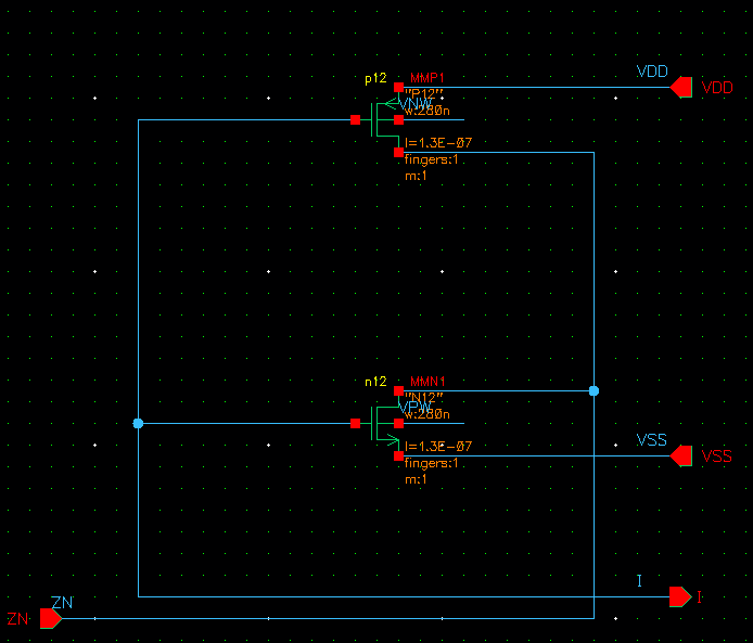
I'm using SMIC0.13um CMOS tech, and its evry kind of std digital cell doesn't connect to power directly. In other words, the well net is isolated within the cell.

for example, here is the schematic of an invertor.
In manual it says we need to add FILLTIE cell to connect wells to power nets. I know that and I did that in the layout.
Wells are connected to the power nets in layout. However, in schematic, just as the pic shows, VPW & VNW are not pins that can be cited outside the std cell. Thus, I cannot connect VPW & VNW from the top level. And that causes the LVS to go wrong: In source there is "I0/VNW""I0/VPW"; but in layout they are directly connected to VDD & VSS, and that is the question.
So how can I fix this difference to clear LVS?
I'm using SMIC0.13um CMOS tech, and its evry kind of std digital cell doesn't connect to power directly. In other words, the well net is isolated within the cell.
for example, here is the schematic of an invertor.
In manual it says we need to add FILLTIE cell to connect wells to power nets. I know that and I did that in the layout.
Wells are connected to the power nets in layout. However, in schematic, just as the pic shows, VPW & VNW are not pins that can be cited outside the std cell. Thus, I cannot connect VPW & VNW from the top level. And that causes the LVS to go wrong: In source there is "I0/VNW""I0/VPW"; but in layout they are directly connected to VDD & VSS, and that is the question.
So how can I fix this difference to clear LVS?

