Continue to Site

Welcome to EDAboard.com

Welcome to our site! EDAboard.com is an international Electronics Discussion Forum focused on EDA software, circuits, schematics, books, theory, papers, asic, pld, 8051, DSP, Network, RF, Analog Design, PCB, Service Manuals... and a whole lot more! To participate you need to register. Registration is free. Click here to register now.

LTSPICE sourse location of a mosfet question

Status
Not open for further replies.

yefj

Advanced Member level 5
Joined
Sep 12, 2019
Messages
1,506
Helped
1
Reputation
2
Reaction score
5
Trophy points
38
Activity points
9,126
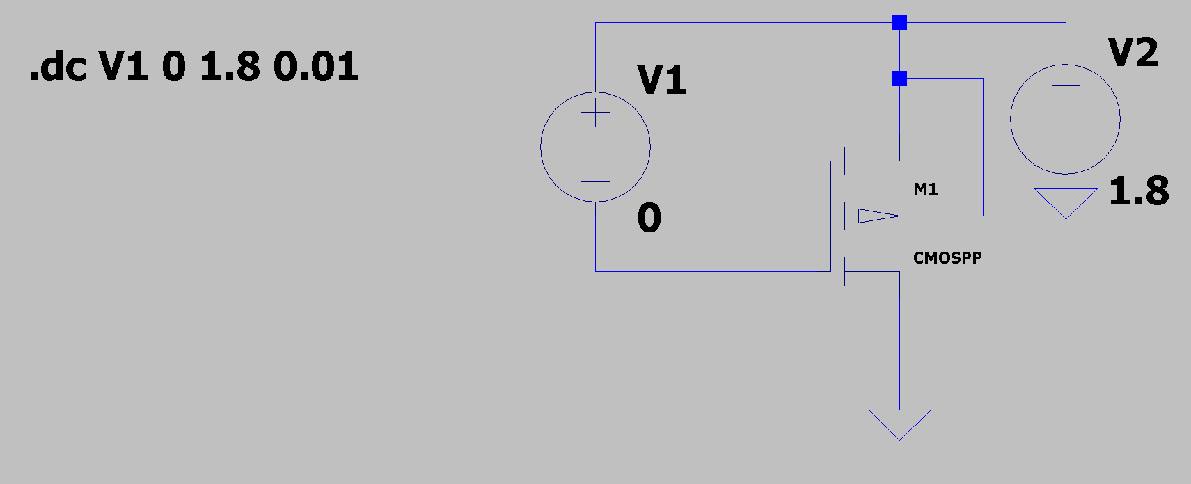
Hello, LTspice is not the real world physics ,Its a netlist thing. I know that NMOS and PMOS have opposite Source location. Generally speaking in real life NMOS and PMOS are simmetric devices and SOURCE and drain are determined by where is the higher voltage. But in LTSPICE i assume its not like in real world :) ? in PMOS we can put the VDS voltage source one way and then to reverse its ,unlike real life the Drain and source will not be switched.

How do i see in LTspice model where is the source of my MOSFET in NMOS and PMOS?
1679746571470.png
 

Suggest to use sources refernced to source node, with a polarity according to normal device notation, as shown below. I noticed you started at least three threads about PMOS biasing, all with confusing source placement and polarity.

As for your question, yes the TSMC MOSFETS are symmetrical, as most planar transistors. The LTSpice symbol has however dedicated S and D pins, suggest to use them as intended. It's indicated by the asymmetrical gate pin.

1679755677844.png
 

Basic IC MOSFETs are symmetric and you can swap the S, D with
no first-order impact. End-fingers, etc. are second order "analog"
concerns.

Power MOSFETs and special FET device structures (extended
drain, LDMOS) are asymmetric and you do care.

If you inspect the symbol at its placed level some schematic tools
will throw a pin ID on hover, or even let you select and inspect
all pin properties. Inspecting at the symbol drawing level can get
you the same if you "flip the symbol in your mind" according to
how-placed.

I prefer to draw my symbols with more explicit labeling. Pin texts
for all terminals, maybe a source arrow instead of body (which is
obvious).

There may be instance properties / checkboxes which enable pin
"features" to display? If so set them on one and then copy it
around.

You could also copy the present symbol to a private library and
edit it to suit your artistic interests.
 

LTspice does simulate the characteristics of real devices.
They include the parasitic substrate diode (an unavoidable part of a real MOSFET) which is connected to the source terminal.
The MOSFETs do conduct equally well in either direction when on (which is used in some circuits, such as to block a reverse polarity connection, or as a synchronous diode in a switching regulator)
In the OFF state they block in the forward direction but will conduct in the reverse direction with the forward drop of the substrate diode.
 

Hello Dick_freebird, i have opened the symbol and i see where is the Source pin as shown bellow.
bellow there is the netlist being used,but the netlist is not specifiend the g s d b pins in it.
how LTspice know how connect my netlist to the pins of the symbol?
how can i update my netlist to specify him the pins so i will see exactly the ltspice connection to the netlist is a perfect fit?
Thanks

1679777777909.png

Code:
.MODEL CMOSPP PMOS (                                LEVEL   = 49
+VERSION = 3.1            TNOM    = 27             TOX     = 4.1E-9
+XJ      = 1E-7           NCH     = 4.1589E17      VTH0    = -0.3906012
+K1      = 0.5341312      K2      = 0.0395326      K3      = 0
+K3B     = 7.4916211      W0      = 1E-6           NLX     = 1.194072E-7
+DVT0W   = 0              DVT1W   = 0              DVT2W   = 0
+DVT0    = 0.5060555      DVT1    = 0.2423835      DVT2    = 0.1
+U0      = 115.6894042    UA      = 1.573746E-9    UB      = 1.874308E-21
+UC      = -1E-10         VSAT    = 1.130982E5     A0      = 1.9976555
+AGS     = 0.4186945      B0      = 1.949178E-7    B1      = 6.422908E-7
+KETA    = 0.0166345      A1      = 0.4749146      A2      = 0.300003
+RDSW    = 198.321294     PRWG    = 0.5            PRWB    = -0.4986647
+WR      = 1              WINT    = 0              LINT    = 2.94454E-8
+XL      = 0              XW      = -1E-8          DWG     = -2.798724E-8
+DWB     = -4.83797E-10   VOFF    = -0.095236      NFACTOR = 2
+CIT     = 0              CDSC    = 2.4E-4         CDSCD   = 0
+CDSCB   = 0              ETA0    = 1.035504E-3    ETAB    = -4.358398E-4
+DSUB    = 1.816555E-3    PCLM    = 1.3299898      PDIBLC1 = 1.766563E-3
+PDIBLC2 = 7.728395E-7    PDIBLCB = -1E-3          DROUT   = 1.011891E-3
+PSCBE1  = 4.872184E10    PSCBE2  = 5E-10          PVAG    = 0.0209921
+DELTA   = 0.01           RSH     = 7.7            MOBMOD  = 1
+PRT     = 0              UTE     = -1.5           KT1     = -0.11
+KT1L    = 0              KT2     = 0.022          UA1     = 4.31E-9
+UB1     = -7.61E-18      UC1     = -5.6E-11       AT      = 3.3E4
+WL      = 0              WLN     = 1              WW      = 0
+WWN     = 1              WWL     = 0              LL      = 0
+LLN     = 1              LW      = 0              LWN     = 1
+LWL     = 0              CAPMOD  = 2              XPART   = 0.5
+CGDO    = 6.35E-10       CGSO    = 6.35E-10       CGBO    = 1E-12
+CJ      = 1.144521E-3    PB      = 0.8468686      MJ      = 0.4099522
+CJSW    = 2.490749E-10   PBSW    = 0.8769118      MJSW    = 0.3478565
+CJSWG   = 4.22E-10       PBSWG   = 0.8769118      MJSWG   = 0.3478565
+CF      = 0              PVTH0   = 2.302018E-3    PRDSW   = 9.0575312
+PK2     = 1.821914E-3    WKETA   = 0.0222457      LKETA   = -1.495872E-3
+PU0     = -1.5580645     PUA     = -6.36889E-11   PUB     = 1E-21
+PVSAT   = 49.8420442     PETA0   = 2.827793E-5    PKETA   = -2.536564E-3
+ NOIMOD=2.0E+00                                NOIA=3.57456993317604E+18                       NOIB=2500
+ NOIC=2.61260020285845E-11     EF=1.1388                                                       EM=41000000 )


the "netlist order" property field will be 1 for D, 2 for G, 3 for S (shown), 4 for B.

In a 3-terminal discrete vertical MOSFET (power devices) B sits inside D and S
inside B, strapped to B.

An integrated planar FET can have a butted & strapped body tie ("tap") or
may have a divorced bodt tie (within some max distance, for effectiveness).
Depending on isolation scheme NMOS B may be common / global (psub!)
orcould be junction or insulator isolated (triple well, SOI). In the SOI case all
FETs are fundamentally 4-terminal (tied or left to float) and in triple well CMOS
your NMOS may be a 5-terminal device.
 

Hello Dick_freebird,looking at my netlist,How can i see the pin order you shown and how many pins are there in the netlist?
Thanks.
 

You don't have a net list, just an instance of the built-in SPICE PMOS model. It matches the 4 pin PMOS symbol, no action of yours required.
 

Hello FVM,I have this model shown bellow.
Its not a subcircuit.so how LTSPICE know how to use properly the model?
This model could be configured for one type of pin connection?
we dont have this line in my spice model.
Syntax: Mxxx Nd Ng Ns Nb <model> [m=<value>] [L=<len>]

https://sanjayvidhyadharan.in/Downloads/tsmc_180_nm/tsmc018.lib

Code:
.MODEL CMOSP PMOS (                                LEVEL   = 49
+VERSION = 3.1            TNOM    = 27             TOX     = 4.1E-9
+XJ      = 1E-7           NCH     = 4.1589E17      VTH0    = -0.3906012
+K1      = 0.5341312      K2      = 0.0395326      K3      = 0
+K3B     = 7.4916211      W0      = 1E-6           NLX     = 1.194072E-7
+DVT0W   = 0              DVT1W   = 0              DVT2W   = 0
+DVT0    = 0.5060555      DVT1    = 0.2423835      DVT2    = 0.1
+U0      = 115.6894042    UA      = 1.573746E-9    UB      = 1.874308E-21
+UC      = -1E-10         VSAT    = 1.130982E5     A0      = 1.9976555
+AGS     = 0.4186945      B0      = 1.949178E-7    B1      = 6.422908E-7
+KETA    = 0.0166345      A1      = 0.4749146      A2      = 0.300003
+RDSW    = 198.321294     PRWG    = 0.5            PRWB    = -0.4986647
+WR      = 1              WINT    = 0              LINT    = 2.94454E-8
+XL      = 0              XW      = -1E-8          DWG     = -2.798724E-8
+DWB     = -4.83797E-10   VOFF    = -0.095236      NFACTOR = 2
+CIT     = 0              CDSC    = 2.4E-4         CDSCD   = 0
+CDSCB   = 0              ETA0    = 1.035504E-3    ETAB    = -4.358398E-4
+DSUB    = 1.816555E-3    PCLM    = 1.3299898      PDIBLC1 = 1.766563E-3
+PDIBLC2 = 7.728395E-7    PDIBLCB = -1E-3          DROUT   = 1.011891E-3
+PSCBE1  = 4.872184E10    PSCBE2  = 5E-10          PVAG    = 0.0209921
+DELTA   = 0.01           RSH     = 7.7            MOBMOD  = 1
+PRT     = 0              UTE     = -1.5           KT1     = -0.11
+KT1L    = 0              KT2     = 0.022          UA1     = 4.31E-9
+UB1     = -7.61E-18      UC1     = -5.6E-11       AT      = 3.3E4
+WL      = 0              WLN     = 1              WW      = 0
+WWN     = 1              WWL     = 0              LL      = 0
+LLN     = 1              LW      = 0              LWN     = 1
+LWL     = 0              CAPMOD  = 2              XPART   = 0.5
+CGDO    = 6.35E-10       CGSO    = 6.35E-10       CGBO    = 1E-12
+CJ      = 1.144521E-3    PB      = 0.8468686      MJ      = 0.4099522
+CJSW    = 2.490749E-10   PBSW    = 0.8769118      MJSW    = 0.3478565
+CJSWG   = 4.22E-10       PBSWG   = 0.8769118      MJSWG   = 0.3478565
+CF      = 0              PVTH0   = 2.302018E-3    PRDSW   = 9.0575312
+PK2     = 1.821914E-3    WKETA   = 0.0222457      LKETA   = -1.495872E-3
+PU0     = -1.5580645     PUA     = -6.36889E-11   PUB     = 1E-21
+PVSAT   = 49.8420442     PETA0   = 2.827793E-5    PKETA   = -2.536564E-3
+ NOIMOD=2.0E+00        NOIA=3.57456993317604E+18        NOIB=2500
+ NOIC=2.61260020285845E-11    EF=1.1388                EM=41000000 )
 

Rule 1: SPICE is stupid. It only knows what you tell it.

The .model statement says "what it is"
The netlist says "what you're doing to it"
The simulation setup says "where to find it"
The simulation results say "what will it do?"

Rule 2: SPICE has layers and sequences of essential events.

The simulator is initialized to its environment (.spicerc, etc.)
The simulator is told what to look at (source the netlist)
The simulator finds all of its referred-to hierarchy through netlisting (or fail)
The human readable netlist is turned into The Matrix of Connectivity
The netlist has delivered simulation parameters, variables, analyses to do
The simulator grinds it out
The simulator executes post-analysis commands to manipulate and display results data


You are at Rule 1(a)
 
  • Like
Reactions: yefj

    yefj

    Points: 2
    Helpful Answer Positive Rating
SPICE has a defined pin order for standard models like NMOS, PMOS, NPN, PNP. It's documented in reference manuals of original Berkley SPICE and any derivate, also LTspice online manual. Therefore it does not appear in the tmsc model. The model is also used in post #2 simulation, as you see assigning it to the LTSpice supplied PMOS symbol gives correct pin order, you don't need to think further about it. Don't edit the predefined symbol pin assignment.
 
  • Like
Reactions: yefj

    yefj

    Points: 2
    Helpful Answer Positive Rating
Status
Not open for further replies.

Similar threads

Part and Inventory Search

Welcome to EDABoard.com

Sponsor

Back
Top