metuo_abeo
Newbie level 5

Hello guys,
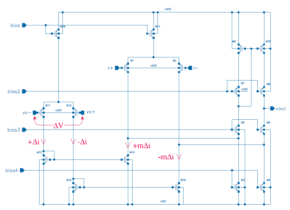
I have to design a low offset voltage auto−zero stabilized CMOS operational amplifier and I started to analyze some existing implementations. I found this one, but I don't understand what are the bias pins (in left, bias 1/2/3/4) and what is their use in the schematic. This internal schematic is the same for both opamps (main and null) in the circuit below (last picture). How can I simulate this opamp?
Do you have any ideas?
Thanks in advance!

