Continue to Site

Welcome to EDAboard.com

Welcome to our site! EDAboard.com is an international Electronics Discussion Forum focused on EDA software, circuits, schematics, books, theory, papers, asic, pld, 8051, DSP, Network, RF, Analog Design, PCB, Service Manuals... and a whole lot more! To participate you need to register. Registration is free. Click here to register now.

Losses on the BJT transitor ?

Status
Not open for further replies.

Coper

Member level 4
Member level 4
Joined
Mar 16, 2017
Messages
69
Helped
0
Reputation
0
Reaction score
0
Trophy points
6
Activity points
773
I may have a slightly strange question.
How to maximize losses on a bipolar transistor?
Let's have this connection
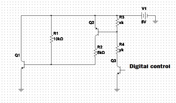
qw.jpg


Q1 is any common transitor with beta about 100
sizes R1 and R2 are given and cannot be changed
We convert a 100 us pulse to Q3 (rectangle or almost saw) and we want to convert as much energy as possible to Q1 into heat for the duration of the pulse.

What should the edge steep pulse, size R3 / R4 look like, so that the losses on Q1 are as large as possible?
The losses will be greatest when the current through R2 is as large as possible for as high as possible or, conversely, when Q1 is opened / close as long as possible
 

Turn on the device to an extent so that it passes some middle amount of current at a middle level of voltage.
Heat dissipated is related to the formula for Watts = V x A.

Notice you can pass high A at low V, which doesn't necessarily generate maximum heat.
Or you can have high V and low A, likewise which doesn't necessarily generate maximum heat.

Therefore you must run tests to find a point somewhere in between the extremes.
 

Hi,

Highest power is with highest current. Thus a high current gain transistor should be used.

If you are free to choose Q1 then I recommend a high power, high current, low R_ds_on logic level Mosfet.
Several hundred Amperes will cause several kW of dissipated power.

Klaus
 

Q. what is this for?

Q1 is always conducting, the 'Digital Control' might make it conduct more if R1 isn't already providing enough base current to saturate it. Ic will already be about hfe * Ib ~ 45mA but isn't limited by any load resistance. Increasing the current may do nothing but destroy Q1.

Brian.
 

This seems like a fun task to figure out. However, there are two several problems as I see it:
  1. The most "POWER" that the bjt can dissipate depends on the characteristics of the battery. If the internal resistance are linear and if the battery symbol is actually representing a DC supply with a resistor in series, then the most power dissipation should be when the voltage drop Vce are half of the battery.
  2. But - since this is an BJT, that's not completely true because ou have to take Ib and Vbe into account and will make the spot slightly different.
  3. If you're only allowed to use that "Digital control", you must disregard #1 and #2 as it gets irellevant.
  4. Because of #3, the most power dissipation possible, you get when the Vce slopes goes straight (no period of stable voltage at all).
  5. Therefore you need to know the slope time for the transistor and use that to calculate the optimal period time to get the condition for maximum slope.
Alternatively - If I where to abuse the transistor this way and find a best approximation, I'd continue from #2 using an opamp to regulate the voltage drop, putting the opamp output between R3/R4 (make sure that the opamp are capable to output enough voltage - use a separate voltage supply as the battery are heavily abused).
 

I'll have to clarify a bit what this is about.
Yes, the transistor has no load and no heatsink. it is not possible to burn through on a large kW mosfet
Let's say the transistor is a 500mW TO92 for example 2N4401
It would be quite difficult to describe the purpose, so I can think of an abstract use .
The transistor serves as a heater and a thermometer at the same time.
We want to keep the PN junction of the transistor at 80C. We know that at a current only through R1, at 80C, the voltage Ube = X and with respect to each degree Celsius increases by 2mV (TC of the semiconductor PN junction) If the temperature drops, we try to heat the transistor more with the help of a pulse through Q2, ie with Q3 = OFF keep the voltage Ube = X. Yes, in the role of the amount of heat supplied, I will read the number of pulses via Q2 / Q3. However, I would still like to know in what shape of the pulse the most energy on the transistor is converted into heat.

In general, will it be the fastest opening / closing of Q2?
or
What if I do slow down the opening and closing of Q2, ie when the shape of the pulse will approach the saw?
I would like to remind you that we are talking about a 100 us pulse and we want to convert as much energy as possible in this pulse into heat (have most mJ of heat)
 

Basically power keeps rising with base current drive.

1616332163767.png


Regards, Dana.
 

I don't know what t think about heating by 5V supply. However, with the new requirements you have informed about, then there gets a couple of needs as I see it:
  • You want to get feedback about Ic.
  • You also need feedback about junction temperature and thereby built in a limitation logic so that the transistor doesn't burn.
  • Since you're spending a lot of load, you should consider including a feedback from battery as well.
 

Hi,

High current..temperature sensing.
Then maybe a darington could be useful.
It increases current gain and additionally increases tempco to 4mV/K.

Klaus
 

If the supply voltage is constant with current, then the maximum transistor power will occur at it's maximum rated current, since the power is simply volts times current.
For example the 2N4401 has a maximum continuous current rating of 600mA, so the dissipation, when ON, would be 0.6A x 5V = 3W.
For a 100us pulse, you could probably go above that value.

For maximum power, you want the transistor to turn on rapidly to it's maximum current, not slowly.

You do realize that R1 keeps Q1 on all the time?
 

If I understand correctly, the idea is that the transistor is deliberately run hot so it works as a heating element. Then somehow the current is either left at nominal (biased through R1) or increased somewhat by adding additional bias current through Q2 & R2. I think it is an unwise strategy, particularly as the transistor will become more conductive by itself as it gets hotter, probably the opposite of what is intended. With no feedback the circuit will not work properly but I wonder if it would be better to use a resistor as the heating element and maybe sense the temperature with a transistor.

Brian.
 
Status
Not open for further replies.

Similar threads

Part and Inventory Search

Welcome to EDABoard.com

Sponsor

Back
Top