Continue to Site

Welcome to EDAboard.com

Welcome to our site! EDAboard.com is an international Electronics Discussion Forum focused on EDA software, circuits, schematics, books, theory, papers, asic, pld, 8051, DSP, Network, RF, Analog Design, PCB, Service Manuals... and a whole lot more! To participate you need to register. Registration is free. Click here to register now.

Logotype/Graphical design on layout

Status
Not open for further replies.

krippkrupp

Newbie level 5
Newbie level 5
Joined
May 31, 2022
Messages
9
Helped
0
Reputation
0
Reaction score
0
Trophy points
1
Activity points
184
When reading the Pulpino datsheet, I noticed that the authors had made a graphical logotype on the layout using cell placement.
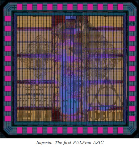
pulpino_layout_logo.jpg

Is there an neat way to do this in SoC encounter during place and route? My thinking is that I can calculate the specific coordinates to describe my logotype and then set the placement density on the board according to the coordinates? Is there a better way to achieve this?

Thank you in advance!
 

Thank you!
Do you know of an easy way to convert a bitmap file to a density screen?
 

long time ago, I created a TCL script to generates the def file to be imported in Innovus.
For the density, I relied on a graphical tool to transform a picture into black and white, or gray and used this value to create a more or less square block in the def file in each sub-"pixel".
--- Updated ---


Status
Not open for further replies.

Part and Inventory Search

Welcome to EDABoard.com

Sponsor

Back
Top