Continue to Site

Welcome to EDAboard.com

Welcome to our site! EDAboard.com is an international Electronics Discussion Forum focused on EDA software, circuits, schematics, books, theory, papers, asic, pld, 8051, DSP, Network, RF, Analog Design, PCB, Service Manuals... and a whole lot more! To participate you need to register. Registration is free. Click here to register now.

[SOLVED] LNA design help,(my stimulation vs real results )

Status
Not open for further replies.

hellotoke

Junior Member level 2
Joined
Sep 26, 2023
Messages
22
Helped
0
Reputation
0
Reaction score
0
Trophy points
1
Activity points
112
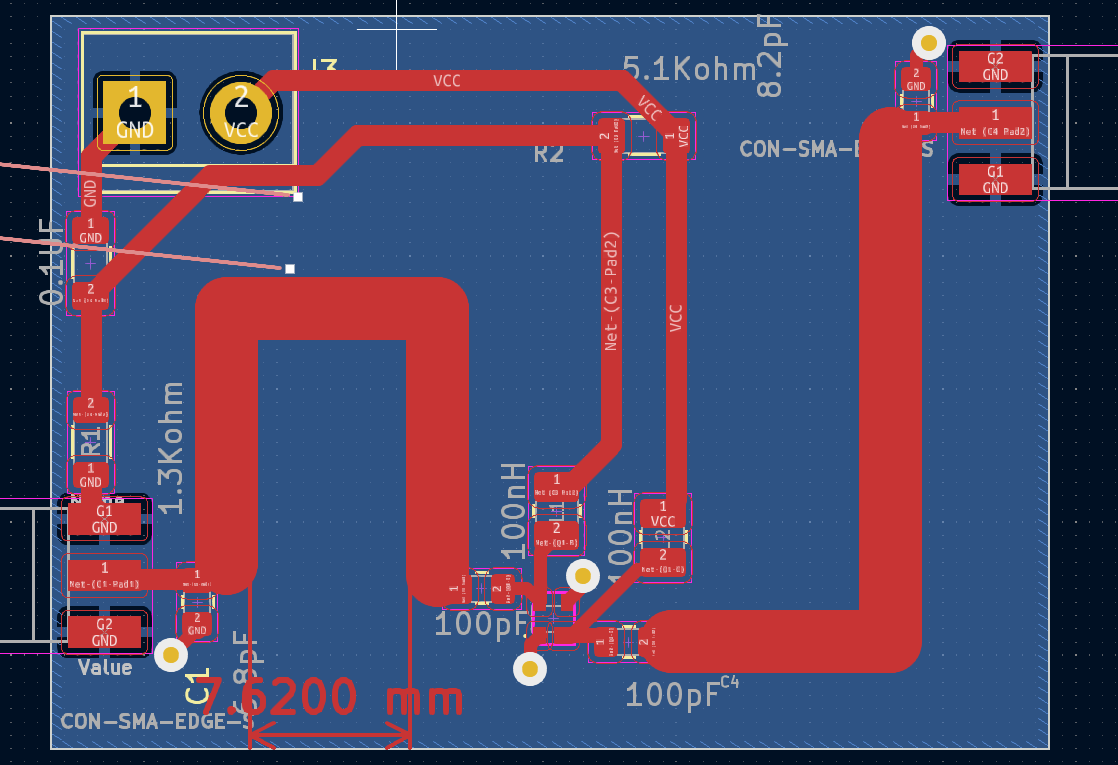
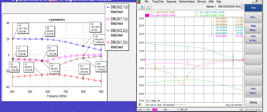
So i built and tested my LNA,these are the results below the gain value at 566MHZ is where i want it to be but the gain at 800MHZ isnt right its way to low compared to the stimulation on the left in awr.Heres my pcb layout on fr4 1.6mm thickness.any help or advice
1695932209601.png

1695932447246.png
 

Hello,

At 800MHz you have a really poor matching (-0.35dB), practically a full reflection. Maybe your problem is in the input matching network. When the signal not enters the amplifier you couldn't have gain. Could you send a schematic of the circuit?

By the waye, where is the LNA located excatly?

Regards
 
This layout is NOT a RF layout. Even-tough the operating frequency is low, the layout is bad.
 

Hello,

At 800MHz you have a really poor matching (-0.35dB), practically a full reflection. Maybe your problem is in the input matching network. When the signal not enters the amplifier you couldn't have gain. Could you send a schematic of the circuit?

By the waye, where is the LNA located excatly?

Regards
1696075311381.png

i matched it at 566 MHZ
 

Status
Not open for further replies.

Similar threads

Part and Inventory Search

Welcome to EDABoard.com

Sponsor

Back
Top