Continue to Site

Welcome to EDAboard.com

Welcome to our site! EDAboard.com is an international Electronics Discussion Forum focused on EDA software, circuits, schematics, books, theory, papers, asic, pld, 8051, DSP, Network, RF, Analog Design, PCB, Service Manuals... and a whole lot more! To participate you need to register. Registration is free. Click here to register now.

LM567 - output triggers during power-on

Paul_V

Newbie level 4
Newbie level 4
Joined
Jul 31, 2024
Messages
7
Helped
0
Reputation
0
Reaction score
0
Trophy points
1
Activity points
43
Hello, everyone.


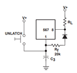
I'm designing a circuit with several LM567 IC's.
It's open-collector output should trigger a logic gate latch and open a lock, once desired frequency is detected.
Using the reference schematic, IC works as expected, turning LED on, when input frequency match.
However, when I power-up the circuit, I'm constantly getting a false trigger. LED turns on momentarily.
This is a problem in my design, because it also triggers the latch during power-up, opening a lock.
Tried adding RC, additional pull-up resistor, darlington, input filtering, soft start, etc.
RC does help, but only for a couple of short power-ups and reduces overall sensitivity of the circuit.

What puzzles me even more, there is a schematic in the datasheet to convert LM567 output to behave as a latch, which also false triggers on power-up.
How can I prevent this power-up trigger?


Thanks a lot in advance.

LM567.PNG
 
Hi,

Link to datasheet?

Klaus

Sorry,
pls see the attachment.

One is from TI, the other is from Phillips (which is considered more thorough)
 

Attachments

  • NE567.pdf
    201.1 KB · Views: 45
  • TI-LM567.pdf
    2.8 MB · Views: 59
Last edited:
Do you know what the output state of th LM567 is on power up? I suspect it’s indeterminate, (probably high impedance), which would look like a momentary high until the device gets going and pulls the output low.

Have you looked at the output with a scope? If there’s a short glitch you might be able to solve the problem with a small RC. Otherwise you may need to add some circuitry to hold off the rest of the circuitry until the LM 567 is stable. Maybe a POR on the latch.
 
Here's the output between pin 8 of the IC and 10k pull-up during power-up.

I've tried several RC combinations, but it does not help when I trigger a power button multiple times, once the capacitor is not fully discharged.
And sometimes the effect is opposite - I get a momentary trigger on power-off.

I guess I'm out of luck?
I could add delay to the logic, but then I don't get the purpose of the latch output circuit in the datasheet if it self triggers on power-up.
Maybe there are, indeed, differences between NE567 and LM567.

UPD: lowering C3 value to 30pf (from initially recommended 2*C2) seem to have reduced this effect significantly.
The power-up curve seems to be directly affected by it.
It is mentioned that if C3 value is too low, chatter may be induced on the output. I'll have to run some tests

photo_2024-07-31_20-37-51.jpg
 

Attachments

  • latch.PNG
    latch.PNG
    8.9 KB · Views: 60
Last edited:
Something like this. The NPN is 567 output transistor. Delay here is ~ 17 mS from first noise pulse..

1722458839484.png


Regards, Dana.
 

Attachments

  • 1722458371791.png
    1722458371791.png
    159.9 KB · Views: 44
The described behaviour is expectable by design due to active low output and filter terminal polarity. To avoid output pulse during power on, connect C3 to V+ rather than ground.
 
I'm a bit confused. You are showing your output jumping high and then decaying to zero. Zero output implies an in-band signal detected. Does that make sense?

And, again, wouldn't it be simpler to just add a long reset signal to the circuit that this is driving so that it will ignore initial glitches?
 
Thanks a lot, everyone, for all your replies.

The described behaviour is expectable by design due to active low output and filter terminal polarity. To avoid output pulse during power on, connect C3 to V+ rather than ground.

Spot-on, that actually made a huge difference! No more power-up triggers and the bandwidth tolerance became even tighter.
And the latch circuit now works flawlessly. There's a short trigger on power-off now, but I think it should not affect anything.

I'm a bit confused. You are showing your output jumping high and then decaying to zero. Zero output implies an in-band signal detected. Does that make sense?

And, again, wouldn't it be simpler to just add a long reset signal to the circuit that this is driving so that it will ignore initial glitches?

The output of the IC is active low (open collector transistor to ground\negative), which I tied to a 10K pull-up resistor and put a probe in between.
So, when signal is detected (or output false triggers) voltage flows from the pull-up through transistor to GND. It can drive up to 100mA, according the the datasheet.

If none of the de-chatter options or skew adjustments help, then you can filter out glitches with a cap load into a hysteresis gate. Then feedback the non-inverted de-glitched output for the latch function.

De-chatter options prevent output flicker upon signal detection while keeping cap values reasonable. No luck in my case, unfortunately.
 
Hi,

there are ready to buy 3 pin RESET circuits, which include a power-ON delay (250 ms or so...)

adding an AND gate to the output will prevent form power ON glitch.

Klaus
 
The output of the IC is active low (open collector transistor to ground\negative), which I tied to a 10K pull-up resistor and put a probe in between.
So, when signal is detected (or output false triggers) voltage flows from the pull-up through transistor to GND. It can drive up to 100mA, according the the datasheet.
Yes, it's active low, which is why I'm confused. Your plot shows the output going low and staying there. That's not a glitch, that would seem to be the wrong state.
 
Yes, it's active low, which is why I'm confused. Your plot shows the output going low and staying there. That's not a glitch, that would seem to be the wrong state.
Perhaps the latched response to an unlatched observation.

I suggest you deflect.

- minimize C3 for glitch duration without compromising PLL performance and feedback the OR’d output of the active low signal and the RC delayed signal.
 
Yes, it's active low, which is why I'm confused. Your plot shows the output going low and staying there. That's not a glitch, that would seem to be the wrong state.

I think I get it now, my bad. Here's another shot.
Pls take my statements with a grain of salt, I'm in no way an expert.

Thanks a lot, everyone. Your advice has been really helpfull.
So far, two ICs do work as intended now.
If everything goes well, I'd like to keep it as simple as possible.
Otherwise, I'll add delay circuit to logic gates.
 

Attachments

  • photo_2024-08-01_12-19-53.jpg
    photo_2024-08-01_12-19-53.jpg
    200.5 KB · Views: 45
Last edited:
I think I get it now, my bad. Here's another shot.
Pls take my statements with a grain of salt, I'm in no way an expert.

Thanks a lot, everyone. Your advice has been really helpfull.
So far, two ICs do work as intended now.
If everything goes well, I'd like to keep it as simple as possible.
Otherwise, I'll add delay circuit to logic gates.
Wait, what? The output is high before you power on? That’s what your plot is showing.
 
This time there's a divider on the output, that is powered by the breadboard.
The IC is powered on by a separate switch.
This way I was trying to compare the glitch duration using different capacitors without having too much bouncing on the scope.

Sorry, I should have specified that.
Most of the parts are already assembled, so I could not redo the exact same test, unfortunately.
 
Ok, so this looks like some function of the chip: when it powers on, it drives its output low for 100uS. You're not going to be able to "filter" that out. You just need to delay the circuit that is being driven by that signal.
 

LaTeX Commands Quick-Menu:

Similar threads

Part and Inventory Search

Welcome to EDABoard.com

Sponsor

Back
Top