Continue to Site

Welcome to EDAboard.com

Welcome to our site! EDAboard.com is an international Electronics Discussion Forum focused on EDA software, circuits, schematics, books, theory, papers, asic, pld, 8051, DSP, Network, RF, Analog Design, PCB, Service Manuals... and a whole lot more! To participate you need to register. Registration is free. Click here to register now.

[SOLVED] level shifter layout, multiple source issue

Status
Not open for further replies.

mssong

Junior Member level 2
Joined
Jul 25, 2023
Messages
22
Helped
0
Reputation
0
Reaction score
0
Trophy points
1
Activity points
181
I'm trying to layout a level shifter.
I know the multiple source warning is fine, but the comparison result doesn't make any sense to me.

Is this a guardring issue by any chance?
I'm wondering what other issues I might have.

Additionally, I'm wondering how the level shifter wraps the guardring.

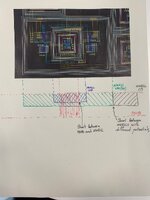
In the following picture, the inside is the pgr guardring and inverter, just outside is the ngr guardring (1.8V), then the next outside is likewise ngr guardring (5V).

Where the ngrs touch each other, the top is 5V and the right is 1.8V.
The layout is clearly correct.

Translated with www.DeepL.com/Translator (free version)

1724961713014.png
 

I do not see an error report (snippet) nor markers nor the
rule's construction / intent.

I could speculate, on no basis whatsoever, that maybe a
triple nested guardring is somehow breaking the logic.
Who does that, this way?

Not knowing fill codes or anything, presuming this is basic
P-substrate JI, are both "VIN" and "VDD" rings trying to
"stamp" bulk psub? Looks kinda like, to me.
1724995059686.png
1724995071072.png

Thank you. The level shifter individual layout works fine, not the whole layout, so I thought it was possible.
The error code is the same as above.

So for the level shifter, the guarding usually only wraps around the outer VIN?
 

Hi @mssong ,

First of all, you layout have a lot of fundamental mistakes. I highly recommend getting yourself familiar with CMOS device cross-sections before doing layout, because it is very important.

1. As @dick_freebird mentioned above, your triple-well structure (PSUB ring, then NWELL om the top of another NWELL) makes completely no sense. You are basically shorting the body connections of your NMOS with PMOS:
1725018715373-jpeg.193435


2. Your PMOS transistors have different body voltages (1.8V and 5V) -> so their NWELLs are not allowed to touch each other, because it will lead to a short between different potentials;
3. Use ERC analysis in Calibre to fix these errors (don't forget to specify power and ground potentials there).

I would recommend practice doing layout of a simple inverter first and make sure that you understand the basics.
Watch a video tutorial, i.e. this one:
Hopefully, that helps.
 

Attachments

  • 1725018715373.jpeg
    1725018715373.jpeg
    126 KB · Views: 64
  • 1725019031717.png
    1725019031717.png
    105.9 KB · Views: 20

Hi @mssong ,

First of all, you layout have a lot of fundamental mistakes. I highly recommend getting yourself familiar with CMOS device cross-sections before doing layout, because it is very important.

1. As @dick_freebird mentioned above, your triple-well structure (PSUB ring, then NWELL om the top of another NWELL) makes completely no sense. You are basically shorting the body connections of your NMOS with PMOS:
1725018715373-jpeg.193435


2. Your PMOS transistors have different body voltages (1.8V and 5V) -> so their NWELLs are not allowed to touch each other, because it will lead to a short between different potentials;
3. Use ERC analysis in Calibre to fix these errors (don't forget to specify power and ground potentials there).

I would recommend practice doing layout of a simple inverter first and make sure that you understand the basics.
Watch a video tutorial, i.e. this one:
Hopefully, that helps.
Thank you very much. I understand perfectly.
 

Status
Not open for further replies.

Similar threads

Part and Inventory Search

Welcome to EDABoard.com

Sponsor

Back
Top