xihuwang
Member level 2

Hi:
A PLL design has big peak to peak jitter.
The designer thinks :
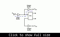
1. The defect of input and output buffer ( ref to pic 1 below, when the
reference frequency is 100MHz, the test result of the peak to peak
jitter of Fref is 680ps)
2. The process variation of the capacitor in loop filter for 90nm
maybe be the reason of large jitter of the pll design .
My questions are :
1. Why and How the defect of buffer can result in the large jitter, and how
to resove the problem( Or how to design the buffer to decrease the jitter)
2. The designer think the other reason lies in the variaton of the filter cap.
But I think maybe the resistor value's variation maybe the reason.
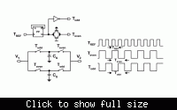
The design use switch cap ckt to work as the resistor in the LPF.
So my question is wheather switch cap resistor can work properly
in PLL. Have you used this kind of SC resistor to decrease chip area?
This question is important for me for it is important for me to find out
a way to implement the resistor instead of physical resistor ( the
target process's sheet resistor is too small)
Thanks forward !


