melkord
Full Member level 3

Hello,
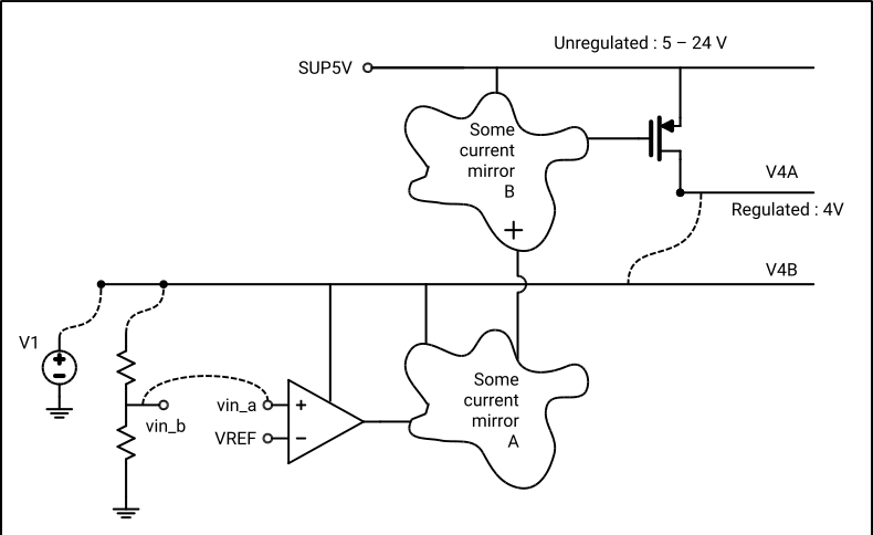
I am designing an LDO whose block diagram looks like the picture below.
The error amplifier is 5 transistor OTA with NMOS diff pair.
All the internal circuits are powered by the output voltage of this LDO, i.e., self powered, V4A and V4B are connected.
At SFF and SFS corners at Temp > 60 degC, the output voltage is pulled up very close to the unregulated VIN, around 4.4V.
I noticed the output of EA is pulled up as well, i.e., the output side PMOS of the PMOS current mirror active load of the OTA goes to triode region.
This makes the current mirror A turns off, but it seems that it is not enough to close the PMOS pass transistor enough.
Is there any thing that I can try to solve this?
