Continue to Site

Welcome to EDAboard.com

Welcome to our site! EDAboard.com is an international Electronics Discussion Forum focused on EDA software, circuits, schematics, books, theory, papers, asic, pld, 8051, DSP, Network, RF, Analog Design, PCB, Service Manuals... and a whole lot more! To participate you need to register. Registration is free. Click here to register now.

LDO immunity from mobile radiation

Status
Not open for further replies.

leo_o2

Advanced Member level 4
Joined
Sep 3, 2004
Messages
1,322
Helped
278
Reputation
558
Reaction score
241
Trophy points
1,343
Location
China
Activity points
5,761
Anyone have gotten idea to improve radiation immunity from mobile phone for LDO? In my LDO design, EMI is poor. When a dailing mobile is close to LDO, LDO's output voltage drop to 0v at 217Hz that is mobile's frequency.
 

A LDO usually has bypass caps at in- and outputs. I shouldn't be too difficult to arrange them in a way, that they are effective at GSM frequencies. If you try to work without bypass caps, it gonna be difficult.
 

If voltage drops to zero, you should broaden your suspicions
to include the shutdown input pin path. Rectified RF ought
to do no more than perturb the analog path slightly.
 

Thanks alot for both of you. Let me describe more details. I designed many LDOs. All LDOs will have bypass cap at input and output. Some LDOs have good RF immunity while some LDOs failed. Recently, we design a PMU chip. Some LDOs in the PMU is good (rising up<100mV during dailing) while some LDOs are poor (drops >1.5V during dailing; drops >2.5V or drops to 0v with mobile dailing at some special directions. The nominal output voltage is 2.8V). We tested it on the same PCB. Input is same node with same input cap close to pins. Output cap is same too. More strange thing is that the circuit structure for both LDO is similar. The good LDO have lower current consumption and the poor LDO burns more quiecent current. The IC layout is different. They are designed by different layout engineers.
 

Once i had very similar problem too. My operational AMP worked as 217Hz detector :) I have solved it with 33pF capacitors on both inputs. I guess it was caused by modem's RF radiated emission. Internal transistor's base was detecting this noise and I saw it on output pin.

In your case, I guess, these voltage drops are caused not by radiated emission, but it depend on the LDO. First has quicker transient response (good dynamic characteristics) and another has slower (not suitable for dynamic load).

-- tantudaisu --
 

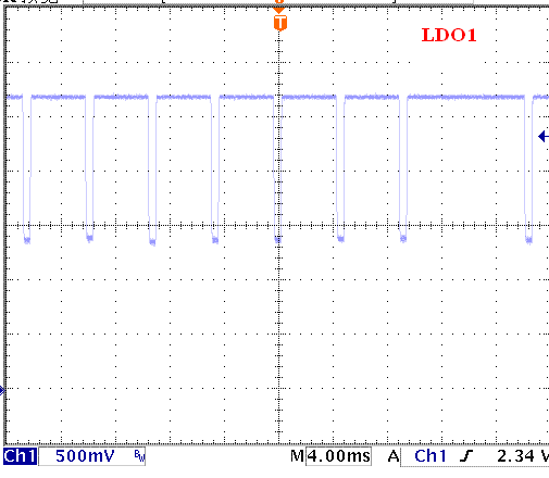
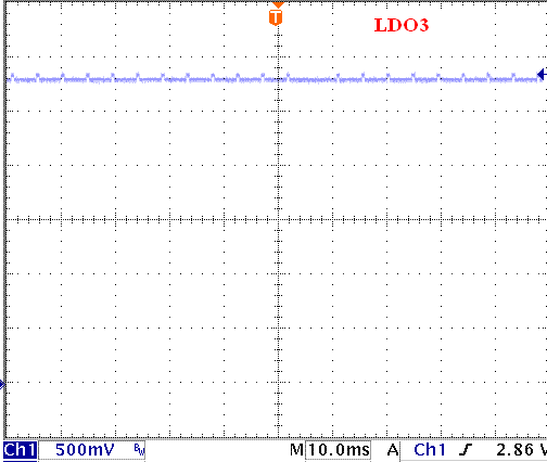
For more details, I post LDO output voltage waveform here. LDO1 nominal output voltage is 2.7V. It drops about 1.4V under mobile radiation. LDO3 nominal output voltage is 2.8V. It rises 50mV under the radiation. LDO1 has similar circuit structure as LDO3. LDO1 quiescent current is 40uA while LDO3 quiescent current is 3uA. Strangely LDO3 have better immunity for the radiation. Both LDOs are implemented in the same PMU chip and are tested with the same PCB board. This phenomenon was verified with several chips. All chips behave same.
49_1292894303.gif
63_1292894303.gif
 

One question that is probably key is "What is the antenna?".

Maybe the fact that the lower current LDOs behave better,
is due to them having less ground current hence higher
imprdance / more filtering against ground perturbations
(the ground plane being probably the single biggest target
for EMI, and not necessarily the same as the LDO reference
return point).

Are these LDOs possibly individually grounded and using a
central or remote reference with its own ground pin?
 

All LDOs ground in the PMU are down bonding to power PAD under the chip. I still suspects IC layout is important for this. These two LDO layout was drawn by two different layout engineers. Some other LDOs in the PMU with same layout behave same.
 

Try to put a 33pF ceramic capacitor between LDO feedback and GND pins (as close as possible).

-- tantudaisu --
 
Last edited:

All LDOs integrate feedback resistor. So add 33pF cap internally at the feedback node? That's huge for IC. However I can have a try next time. Would you pls explain the reason?
 

Semiconductors are always a source of RF demodulation. Each semiconductor (e.g. diodes) needs to be RF-decoupled using a capacitor from 10 to 33pF. EMI capacitors for GSM 900/1800MHz bands (12…18pF + 33pF). On the PCB, these capacitors shall be placed close to the semiconductor and/or input pins.

- tantudaisu -
 
  • Like
Reactions: leo_o2

    leo_o2

    Points: 2
    Helpful Answer Positive Rating
Thanks to tantudaisu. Did you have experiement on this? How to calculate the cap value (33pF) for GSM frequency (900/1800MHz)? Only to add 33pF cap for LDO input node, Feedback node, and output node? Any other internal nodes also need this cap? For examples, the reference voltage for LDO error amplifier, current bias nodes?
 

Usually two capacitors in parallel are used: 33pF for 900MHz band, and 10pF for 1800MHz band. 1800MHz has lower emitting power, so in some cases 33pF is enough. Amp's inputs, FET gates, reference and feedback pins are most sensitive nodes. You have to experiment... Every design is unique... And don't forget, as close as possible!

- tantudaisu -
 

Perhaps you want to inject small stimuli at each node, or each
node with a significant plate area or wire length, and gauge the
response. I have done this for debugging other sorts of
misbehavior. you can make voltage sources with their values
being complex expressions - e.g. ampl=rf_ampl*(rf_node=123) -
and propertize each source (I might recommend you work with
sinusoid current sources that start after delay, so the DC
solution is not whacked) with its unique node assignment,
and index the "pointer" variable in Parametric Analysis (for
Cadence; an alter command, in other SPICEs?). Then you
run the rack of sources and plot the results overlaid, any
sensitive nodes will jump right out at you.

However I have yet to see any mention of the simplest and
most basic thing - scope traces of all the involved pins
(VIN, SHDN, GND, FB, VREF if available) at a timebase about
10X the RF period and 10X the RF envelope period. Until you
know this is or is not a conducted-susceptibility problem,
you don't know whether to look inside the IC or outside for
the solution. The output pin is most likely (but not necessarily
exclusively) a result; you have to identify the input.
 

In my experiement, adding 33pF to input and output didn't reduce the voltage drop. But adding a magnetic bead at the ground pin will reduce it.
 

Status
Not open for further replies.

Part and Inventory Search

Welcome to EDABoard.com

Sponsor

Back
Top