Continue to Site

Welcome to EDAboard.com

Welcome to our site! EDAboard.com is an international Electronics Discussion Forum focused on EDA software, circuits, schematics, books, theory, papers, asic, pld, 8051, DSP, Network, RF, Analog Design, PCB, Service Manuals... and a whole lot more! To participate you need to register. Registration is free. Click here to register now.

ldo buffer design issue, pls help

Status
Not open for further replies.

samuelyou

Newbie level 4
Newbie level 4
Joined
Jul 7, 2010
Messages
6
Helped
0
Reputation
0
Reaction score
0
Trophy points
1,281
Location
china shanghai
Activity points
1,333
I would like to design a ldo with buffer, but some strange thing happened when I added the buffer. The phase margin is ok, but the transient simulation result show the output is oscillation. When I change the buffer to a VCVS, the transient oscillation disappear.

Please help to analysis why the transient oscillation. Thanks!

Added after 6 minutes:

samuelyou said:
I would like to design a ldo with buffer, but some strange thing happened when I added the buffer. The phase margin is ok, but the transient simulation result show the output is oscillation. When I change the buffer to a VCVS, the transient oscillation disappear.

Please help to analysis why the transient oscillation. Thanks!

Added after 6 minutes:

samuelyou said:
I would like to design a ldo with buffer, but some strange thing happened when I added the buffer. The phase margin is ok, but the transient simulation result show the output is oscillation. When I change the buffer to a VCVS, the transient oscillation disappear.

Please help to analysis why the transient oscillation. Thanks!
 

If your dominant pole is the load C and output R, the vcvs changes
all that with its zero output impedance.

Try a realistic series resistance after the vcvs and see if this is the
mechanism.
 

yxo said:
1. I believe you use VCVS with gain 1, don´t you?

yes, I use the VCVS with gain 1. But I confused with the STB simulation result, the phase margin is enough, why the output oscillate? I thought about the slew rate of the EA and the buffer, it seems that the buffer can not follow the EA_out quickly. So I change the buffer to a VCVS.

Added after 10 minutes:

dick_freebird said:
If your dominant pole is the load C and output R, the vcvs changes
all that with its zero output impedance.

Try a realistic series resistance after the vcvs and see if this is the
mechanism.


Sorry, I'm not very clear with this architecture. In my opinion, the dominant pole is the N4 node, one side of the Cc. I would like to use a buffer to seperate the high impendance node and the high parasitic cap node. But the transient oscillation happened, though the STB(cadence spectre) show the phase margin is enough. I really don't know what happened.
 

I don't like how you have attached Cc in the ldo2 schematic,
it's pushing against the low source impedance of M3 and could
be a lot less effective than a more usual M3.D/M5.D connection.
Additionally M3 is going to exhibit a rectifying large signal
behavior, even if it passes the feedback OK at small signal.
As soon as you lose linearity you lose small signal paradigm
validity.

You should look at this aspect, large signal (transient) vs small
signal stability. It's hassled me on more than one regulator /
reference design.
 

    samuelyou

    Points: 2
    Helpful Answer Positive Rating
dick_freebird said:
I don't like how you have attached Cc in the ldo2 schematic,
it's pushing against the low source impedance of M3 and could
be a lot less effective than a more usual M3.D/M5.D connection.
Additionally M3 is going to exhibit a rectifying large signal
behavior, even if it passes the feedback OK at small signal.
As soon as you lose linearity you lose small signal paradigm
validity.

You should look at this aspect, large signal (transient) vs small
signal stability. It's hassled me on more than one regulator /
reference design.

Thanks for all your help! Do you have some papers about the large signal vs small signal stability? If you are convenient, pls share some, thank you!
 

If your using Cadence and doing STB analysis, check the gain margin, if it is less than 10dB then this maybe the cause of the oscillations
 

mnouraldin said:
If your using Cadence and doing STB analysis, check the gain margin, if it is less than 10dB then this maybe the cause of the oscillations

Thanks for your reply, I will check the gain margin.

Added after 7 minutes:

rajanarender_suram said:
Can i see what kind of oscillations u are getting???

The waveform looks like a trangle rather than a sine wave. And the EA works like a comparator, the output is always saturate. The buffer(source follower) output cannot follow the EA output very well.
Thanks for your reply.

Added after 4 minutes:

When I add a small capacitor to EA output node, the oscillation is disappeared. Or I change the Cc(Miller compensation cap) to the EA output, the same thing happened. So I tried to decrease the slew rate of the EA, the oscillation will decrease.
 

HI

cant say if this is gonna help you ...
but the buffer architecture you are using is called Super Source follower.

You can read aboout it in Gray&Meyer's book. There they have also discussed about its instability.(You can see that it is using shunt feedback to reduce the output impedence)

I have used this circuit.. and needs to be designed carefully.
 

On another note... more towards debugging ur problem.

Did you check the stability of your feedbck loop in the voltage buffer.
Since you are driving a capacitive load and the buffer has negative feedback involved you need to ensure its stability as well.

Your stability analysis of outer loop will not reflect that.
you have to check them seperatly
 

I have encounter the same problem ,anyone can tell me how to check the stability of the feedback loop in the buffer?
 

Please try to break the loop at different nodes for stability simulation. If there are several feedback loops, you should check several different ways for loop breaking.
 
thank you for you guys' reply.I tried what you said ,but problem is still alive.so......
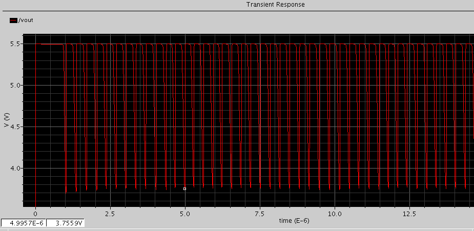
I want to get 5v when input is above 5.5v and the max output current is 50mA,the schematic is same with samuelyou's.when run the ac simulation,the PM and GM are ok,BUT when run transient simulation,the ouput is oscillate.
79_1304843451.png

the load is only a 100k resistor with out a capacitor,and I found the PM of the super buffer is very well.
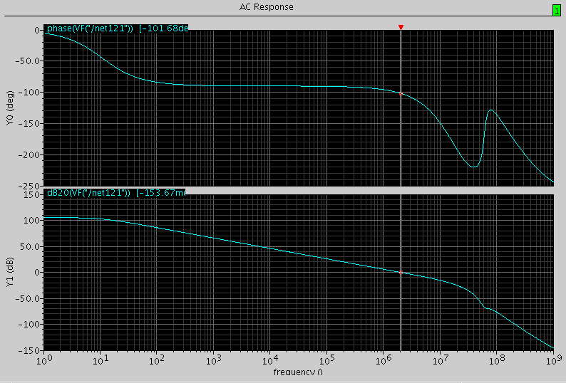
The ac simulation results are show below:
45_1304844076.png

who can help me?

---------- Post added at 09:47 ---------- Previous post was at 09:44 ----------

and the GM is about -20db.

---------- Post added at 09:52 ---------- Previous post was at 09:47 ----------

the GM is about -20db
 

Did you use "stb" analysis? It is more accurate than "AC" analysis.
Where did you break the loop?
Pls also try to break the loop at N5, or N1, or N2. There are more than two loops. Stability is complex.
 

I am confused that all trsistors are saturate in AC simulation but someone cutoff in Transient simulation,but the spice tell me they have the same DC node voltage .When run AC simulation ,I break the loop at N5.
why this happen?
 

Did you have same condition (like load condition) for AC and transient simulation?
You must have same operating point for both AC and transient simulation.
How do you break the loop for AC simulation?
The loop breaking method should remain same DC point to be correct.
Pls post the schematic for AC simulation.
 

Status
Not open for further replies.

Similar threads

Part and Inventory Search

Welcome to EDABoard.com

Sponsor

Back
Top