Vermes
Advanced Member level 4

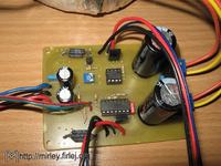
The system is an ordinary regulated power supply built on a rather old stabilizer uA723. The power supplies symmetrical output voltage 3,3-2,6V and current up to 3A. Exceeding the maximum current will cut off the output transistors, which can be treated as overcurrent protection. Direct regulation is subject to positive voltage, while the negative part follows the positive thanks to the system built on the amplifier TL081.
Most of the systems are powered by a single voltage, but described system should be available in every workshop. It is especially useful for analog designs using operational amplifiers or pre-launch the power amplifiers. The advantage of the structure is a very low cost, which 90% is represented by the AC transformer. After completing the power with systems for measuring voltage and current, described power supply becomes a very useful lab instrument.
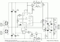
The main element is stabilizer U1 (uA723), which is a precision voltage regulator circuit. This system contains a temperature-compensated reference voltage source, error amplifier and the output transistor that allows the current flow up to 150mA. U1 system works in a typical configuration, in which the internal error amplifier compares the voltage from the divider R0 (5,6k)- R3 (4,7k) with the voltage on the power supply output. Resistors R4 (220R) and R5 (6,8k) and potentiometer P1 (50k) provide respective fraction of the output voltage for the inverting input in the error amplifier U1. Presented here negative feedback loop forces such control at the error amplifier output, so thanks to the regulatory elements R1 (560R), T1 (BD911) and T2 (BD139), the voltage at the output achieved the appropriate value. Voltage from slider P1 will be aligned with the voltage of the divider R0 – R3 in at steady state, so turning the potentiometer we force the output voltage of such value that the slider remains at the same potential all the time. Turning the potentiometer in the direction of the resistor R4 decreases the output voltage. Multiturn potentiometer can be used in the role of the P1, what enables accurate voltage regulation. Another method is to use two potentiometers: one small and one high value. Potentiometer of small value in this case will be used to regulate the exact voltage.
Resistor R2 (0,2R/5W) with transistor T6 (BC548) works as overcurrent protection (current limit). If the AC current taken increases, the voltage drop on R2 also increases. Opening transistor T6 with a voltage drop of approximately 600mV causes a short circuit between the emitter and base of control transistors, and thus reduce the current through T1. Another feedback works here, and the current will be limited to about 0,6/R2, which in this case gives 3A. The resistor value should be chosen, having regard to the transformer used and its performance. In the role of T1 in most cases you will need to use several transistors connected in parallel, to distribute the flowing current and power dissipation for a few transistors.
Operational amplifier U2 (TL081) is directly responsible for the negative half of control. Its output directly controls transistors T3 (BD140) and T4 (BD912). Resistor R9 (560R) limits the current of base T3, acting a similar role to R1 in the positive half of the power supply. Divider R6 (100k), R7 (100k) and P2 (10k) is chosen in such a way that the steady state on the slider P2 there was the ground potential. The voltage increase at the output of the positive half of the power supply will result in increasing the capacity on the slider of potentiometer P2. Amplifier U1 at the same time aiming to align the potential for both outputs will reduce the negative power supply through regulatory elements T3 and T4. The voltage at the negative half will follow the positive, as long as the divider R6, R7, P2 will be set to 1:1 division. Transistor T5 (BC557) limits the current in the negative half of the power supply in the same way as described earlier T6 in the positive half. The maximum value of current in this case is 0,6/R8.
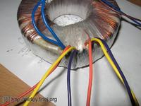
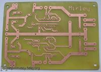
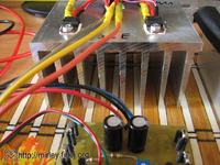
Two independent windings of the power transformer should be connected to sockets IN1 (ARK) and IN2 (ARK). Voltage will be rectified in bridges Br1 (5A) and Br2 (5A) and will be filtered through a capacity C1, C2 (4700uF) and C3, C4 (100nF), and then goes directly to the main transistors T1 and T4 (each of them in practice may consists of multiple transistors connected in parallel). At the output, capacitors C6, C7 (470uF) and C9, C10 (100nF) filter the voltage. The power output is OUT connector (ARK), on which there is available adjustable symmetrical voltage in relation to the mass. Additionally, it is possible to solder dividers R10-R13 on the board, to measure the output voltage by means of a microcontroller with ADC converter. This solution allows you to quickly make a voltage indicator.

Link to original thread (useful attachment) – Laboratoryjny Zasilacz Symetryczny 3,3-26 V